SDRAM Controller
3-74 ADSP-21368 SHARC Processor Hardware Reference
SDRAM Timing
To support key timing requirements and power-up sequences for different
SDRAM vendors, the SDC provides programmability for t
RAS
, t
RP
, t
RCD
,
t
WR
and the power-up sequence mode.
CAS latency is programmed in the
SDCTL register based on the frequency
of operation. (Please refer to the SDRAM vendor’s data sheet for more
information.)
For other parameters, the SDC assumes:
• Bank cycle time is t
RC
= t
RAS
+ t
RP
• Bank A to Bank B cycle time is t
RRD
= t
RCD
+ 1 (ADSP-2137x
processors only)
• Refresh cycle time is t
RFC
= t
RAS
+ t
RP
• Exit self-refresh time is t
XSR
= t
RAS
+ t
RP
• Load mode register to activate time is t
MRD
= 2 SDCLK cycles.
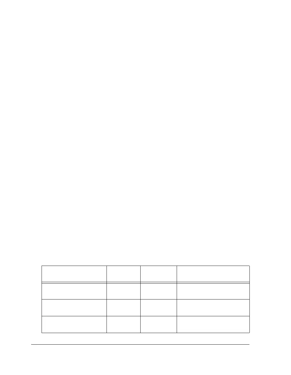
Table 3-27 and Table 3-28 show the optimal data throughput for 32- and
16-bit data accesses respectively. Table 3-29 shows accesses between exter-
nal memory banks.
Table 3-27. Optimal Data Throughput for 32-Bit Data Accesses
(CAS Latency = 2)
Access Operation Page Throughput per SDCLK
(32-Bit Data)
Sequential and
uninterrupted
Read Same 32 words per 37 cycles
Any Write Same core = 1 word per cycle
DMA = 1 word per 2 cycles
Non Sequential and
uninterrupted
Read Same 6 cycles
 Loading...


