ADSP-21368 SHARC Processor Hardware Reference A-21
Register Reference
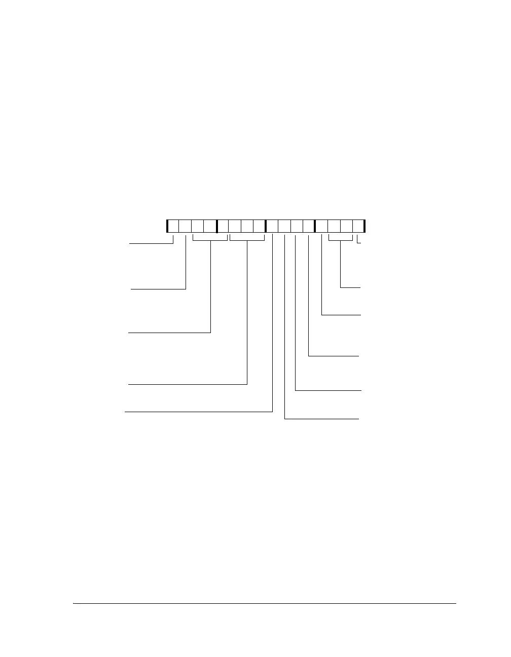
SDRAM Control Register (SDCTL)
The SDRAM memory control register includes all programmable parame-
ters associated with the SDRAM access timing and configuration. This
32-bit register is located at address 0x1800 and is shown in Figure A-8
and described in Table A-6. For more information, see “SDRAM Control
Register (SDCTL)” on page 3-39.
Figure A-8. SDRAM Control Register (Bits 16–31)
31 30 29 28 27 26 24 23 22 21 20 19 18 17 16
0000000000000000
SDBUF
Row Address Width
000=8, 001=9
010=10, 011=11
100=12, 101=13
110=14, 111=15
X16DE
SDRAM External Data Path Width
(ADSP-21371 only)
1=16 bits
0=32 bits
SDRAW
SDRAM tRCD Specification
tRCD = 1–7 SDCLK cycles
SDTWR
SDRAM tWR Specification
tWR = 1–3 SDCLK cycles
NO BSTOP
25
SDORF
Pipeline Option with External Register Buffer
1=External SDRAM CTL/ADDR control buffer enable
0=No buffer option
Force AR
Optional Refresh
1=Auto refresh not performed
0=Auto refresh occurs when
refresh counter expires
Force Auto Refresh
1=Force auto refresh
0=No effect
Force PC
Force Precharge
1=Force precharge
0=No effect
STDRCD
Force LMR
SDCTL (0x1800)
Disable
1=Disable burst stop
0=Issue burst stop on a
read/write break
PGSZ 128
Disable
1=Page size is 128 words
(Col width = 7 bits)
0=No effect
Force Auto Refresh
1=Force mode register write
0=No effect
 Loading...


