External Memory Interface
3-16 ADSP-21368 SHARC Processor Hardware Reference
L
For the ADSP-21371 processor, the SDCTL register needs to be
explicitly programmed for 16-bit wide external memory by setting
bit 16 (X16DE) of this register.
EMI Registers and Signals
The external port global control register is used to set the priority between
core and DMA memory accesses and to determine whether SDRAM or
asynchronous memory is used on each bank. The bits in this register are
described in Table 3-7.
In multiple clock domains, the effect latency of the control register bits of
the external port varies. The worst case is 1:4, where the time from a con-
trol bit write, to the time the write takes effect, is a maximum of four IOP
clock cycles/eight core clock cycles. It is essential to put NOP commands
(no operation) in the program to accommodate this time. It is also advised
that programs not perform any external memory accesses until the effect
takes place. The status bits of the control register can also have a maxi-
mum latency of up to one cycle.
L
The EPCTL register bits should not be changed during external
accesses.
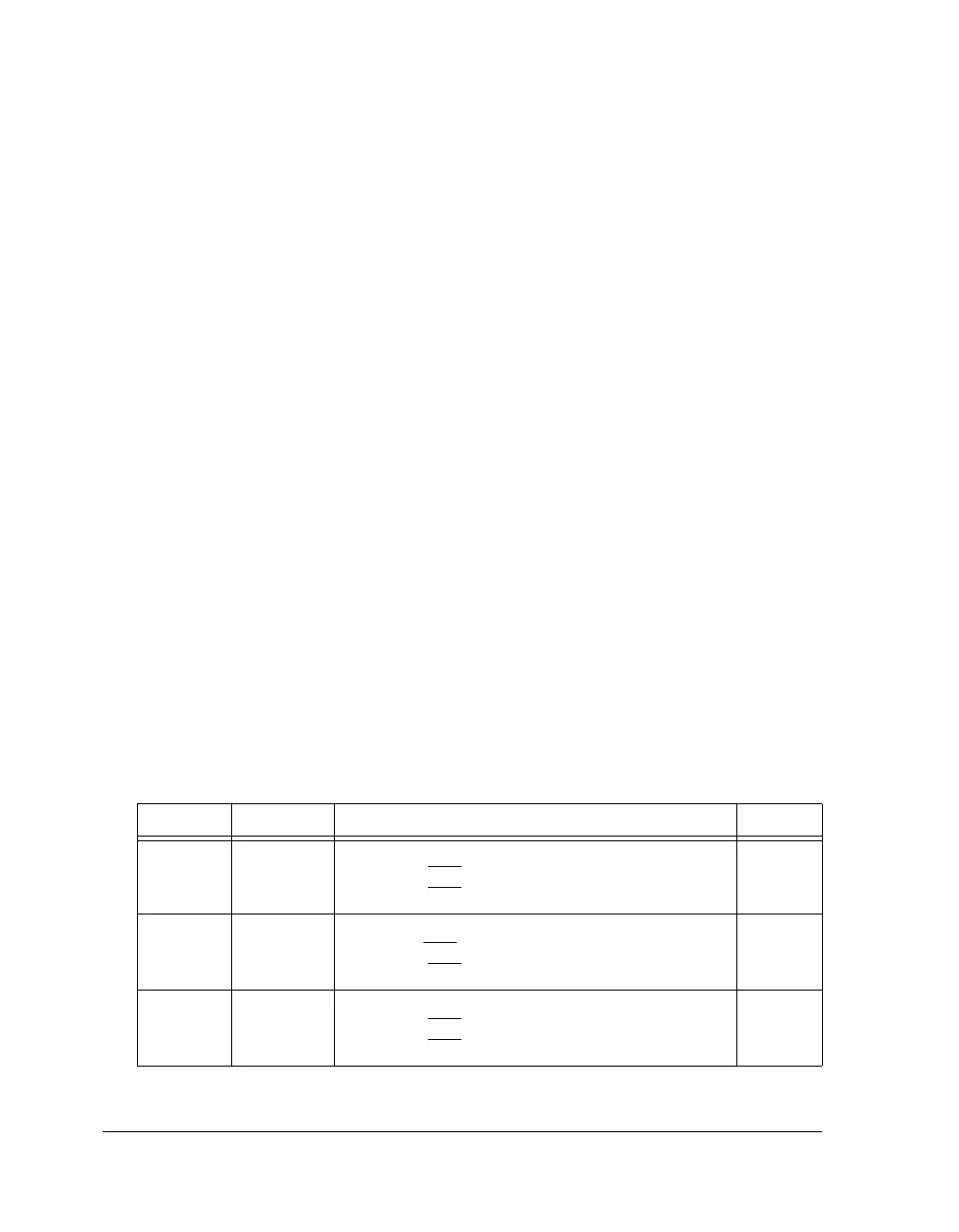
Table 3-7. External Port Control Register Bit Descriptions
Bit Name Description Default
0B0SDBank 0 SDRAM.
1 = Bank 0 (MS0
) connected to SDRAM
0 = Bank 0 (MS0
) connected to asynchronous memory
0
1B1SDBank 1 SDRAM.
1 = Bank 1(MS1) connected to SDRAM
0 = Bank 1 (MS1
) connected to asynchronous memory
0
2B2SDBank 2 SDRAM.
1 = Bank 2 (MS2
) connected to SDRAM
0 = Bank 2 (MS2
) connected to asynchronous memory
0
 Loading...


