UART Control and Status Registers
A-128 ADSP-21368 SHARC Processor Hardware Reference
DMA Control Registers (UARTxTXCTL, UARTxRXCTL)
Use these registers (described in Table A-49 and Table A-50) to enable
DMA, DMA chaining, and to clear the transmit and receive buffers. The
transmit and receive registers are read-write registers and their addresses
are:
UART0TXCTL – 0x3F04
UART1TXCTL – 0x4304
UART0RXCTL – 0x3E04
UART1RXCTL – 0x4204
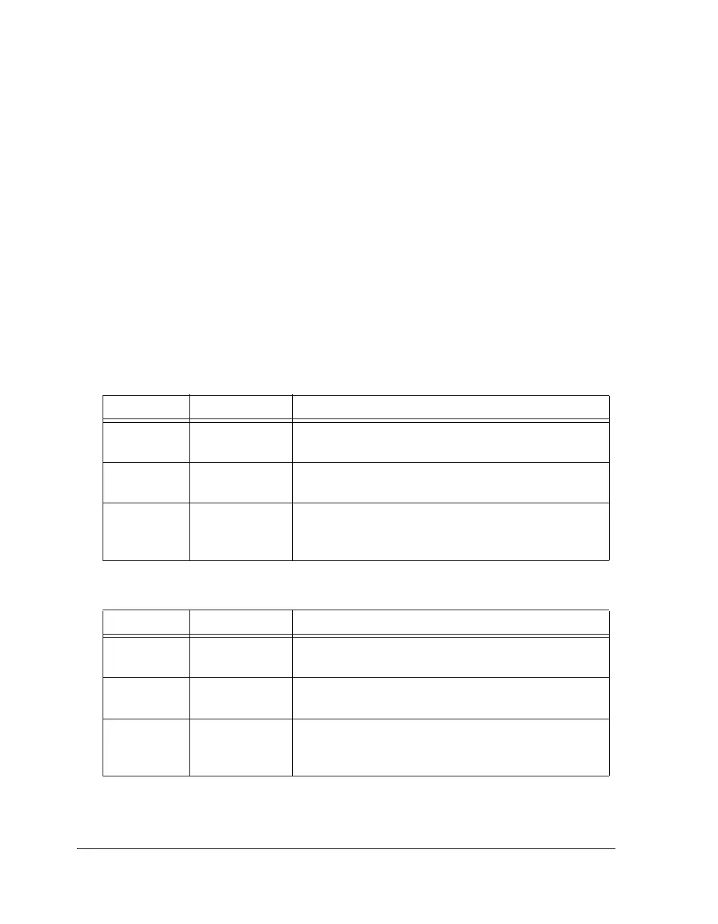
Table A-49. UARTxTXCTL Register Descriptions
Bit Name Description
0UARTENDMA Transmit Buffer Enable. When set (=1), enables the
transmit buffer. When cleared, clears the transmit buffer.
1UARTDENDMA Enable. When set (=1), enables DMA on the speci-
fied channel. When cleared, disables DMA.
2UARTCHENChain Pointer DMA Enable. When set (=1), enables chain
pointer DMA on the specified channel. When cleared, dis-
ables chained DMA.
Table A-50. UARTxRXCTL Register Descriptions
Bit Name Description
0UARTENDMA Receive Buffer Enable. When set (=1), enables the
receive buffer. When cleared, clears the receive buffer.
1UARTDENDMA Enable. When set (=1), enables DMA on the speci-
fied channel. When cleared, disables DMA.
2UARTCHENChain Pointer DMA Enable. When set (=1), enables chain
pointer DMA on the specified channel. When cleared, dis-
ables chained DMA.
 Loading...


