Signal Routing Units
4-8 ADSP-21368 SHARC Processor Hardware Reference
Signal Routing Units
This section describes how to use the signal routing units (SRU1 and
SRU2) to connect inputs to outputs.
Connecting Peripherals
The SRUs can be likened to a set of patch bays, which contains a bank of
inputs and a bank of outputs. For each input, there is a set of permissible
output options. Outputs can feed to any number of inputs in parallel, but
every input must be patched to exactly one valid output source. Together,
the set of inputs and outputs are called a group. The signal’s inputs and
outputs that comprise each group all serve similar purposes. They are
compatible such that almost any output-to-input patch makes functional
sense.
Table 4-2 lists the SRU signal groups that are named sequentially A
through F for SRU1 and A through C for SRU2. Each group routes a
unique set of signals with a specific purpose. For example, SRU1 Group A
routes clock signals, while SRU2 group A routes the external 14 pins and
other sources like timer outputs to the inputs of the various peripherals.
Unlike SRU1 in the DAI module, all types of functionality like serial
clock and data are clubbed into the same group in the DPI/SRU2.
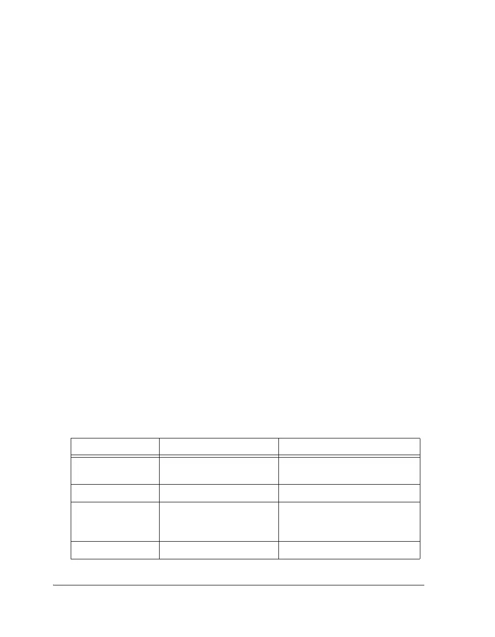
Table 4-2. Pin Signal Group Assignments
Signal Group DAI (SRU1) DPI (SRU2)
Group A Clock routing control Input routing control, includes serial
clock and data
Group B Serial data routing control Pin signal assignments
Group C Frame sync routing control Pin enable assignment, routes enables
of various peripherals to the drive
buffer of each of the 14 pins
Group D Pin signal assignments N/A
 Loading...


