Clock Derivation
14-20 ADSP-21368 SHARC Processor Hardware Reference
RESET and CLKIN
The processor receives its clock input on the CLKIN pin. The processor uses
an on-chip, phase-locked loop (PLL) to generate its internal clock, which
is a multiple of the CLKIN frequency. Because the PLL requires some time
to achieve phase lock, CLKIN must be valid for a minimum time period
during reset before the RESET signal can be deasserted. For information on
minimum clock setup, see the appropriate ADSP-2136x or ADSP-2137x
SHARC processor data sheet.
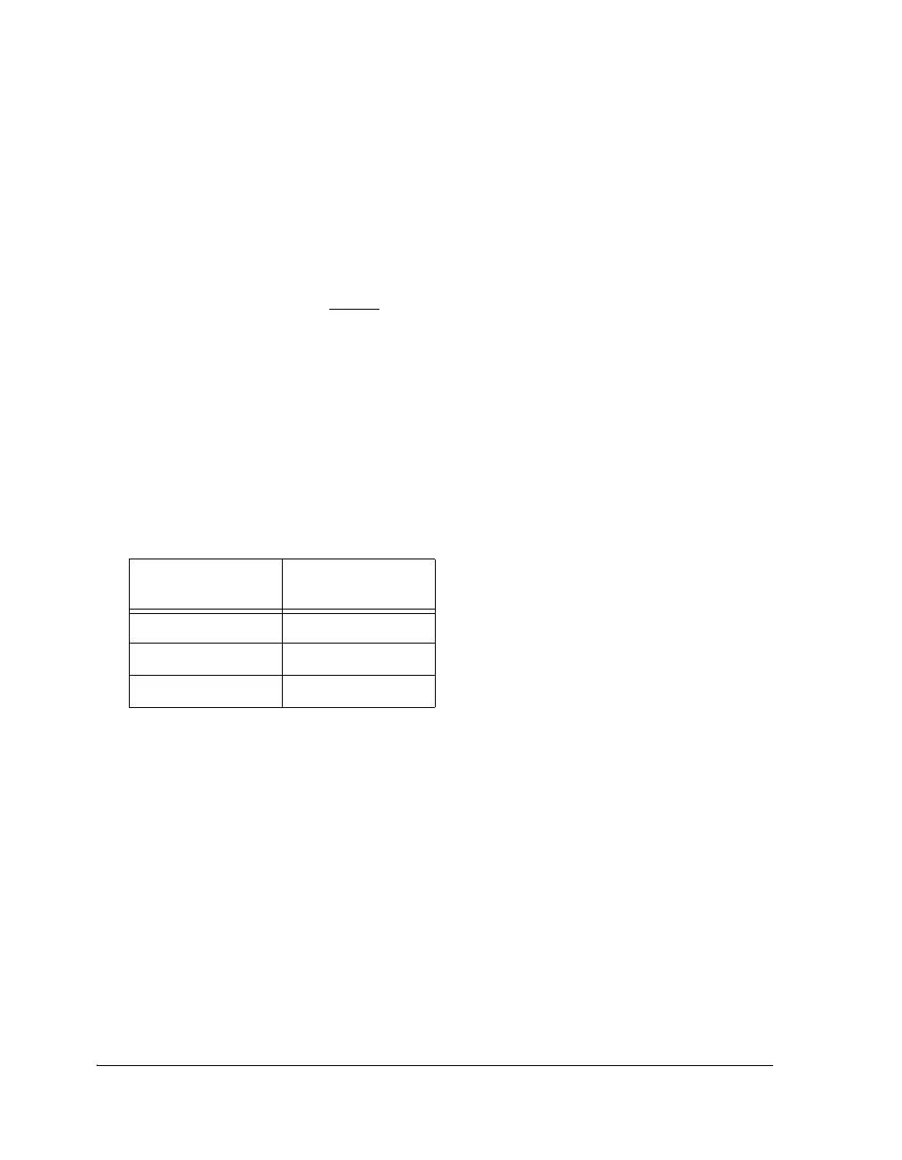
Table 14-2 describes the internal clock to CLKIN frequency ratios sup-
ported by the processor. Note that programs control the PLL through the
PMCTL register. For more information, see “Power Management Control
Register (PMCTL)” on page A-170.
L
When using an external crystal, the maximum crystal frequency
cannot exceed 25 MHz. The internal clock generator, when used in
conjunction with the
XTAL pin and an external crystal, is designed
to support up to a maximum of 25 MHz external crystal frequency.
For all other external clock sources, the maximum CLKIN frequency
is 50 MHz.
Table 14-3 demonstrates the internal core clock switching frequency
across a range of CLKIN frequencies. The minimum operational range for
any given frequency may be constrained by the operating range of the
phase-lock loop. Note that the goal in selecting a particular clock ratio for
Table 14-2. Pin Selectable Clock Rate Ratios
CLKCFG1-0 Core to CLKIN
Ratio
00 6:1
01 32:1
10 16:1
 Loading...


