ADSP-21368 SHARC Processor Hardware Reference 14-21
System Design
the application is to provide the highest permissible internal frequency for
a given
CLKIN frequency. For more information on available clock rates,
see the processor-specific data sheet.
L
Shared memory processor designs that use several ADSP-21368
processors must have the same CLKIN source. These devices should
also be brought out of reset together.
If an external master clock is used, it should not drive the CLKIN pin when
the processor is not powered. The clock must be driven immediately after
power-up; otherwise, internal gates stay in an undefined (hot) state and
can draw excess current. After power-up, there should be sufficient time
for the oscillator to start up, reach full amplitude, and deliver a stable
CLKIN signal to the processor before the reset is released. This may take
100 μs depending on the choice of crystal, operating frequency, loop gain
and capacitor ratios. For details on timing, refer to the processor-specific
data sheet.
After the external processor RESET signal is deasserted, the PLL starts oper-
ating. The rest of the chip is held in reset for 4096 CLKIN cycles after RESET
is deasserted by an internal reset signal. This sequence allows the PLL to
lock and stabilize. Add one CLKIN cycle if RESET does not meet setup
requirements with respect to the
CLKIN falling edge.
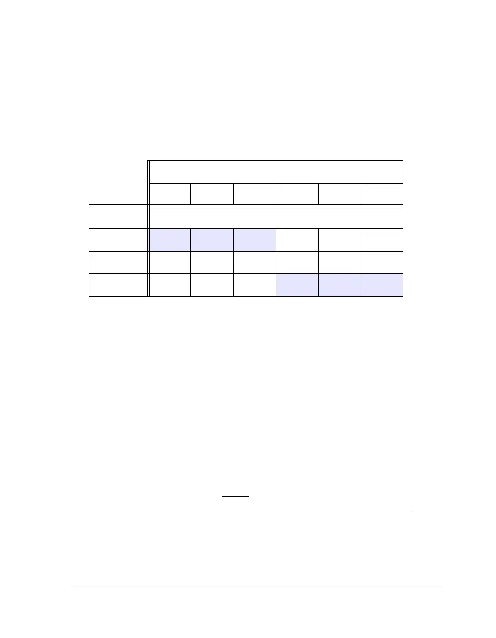
Table 14-3. Selecting Core to CLKIN Ratio
Typical Crystal and Clock Oscillators Inputs
12.500 16.667 25.000 33.333 40.000 50.000
Clock Ratios Core CLK (MHz)
3:1
N/A N/A N/A 100.000 120.000 150.000
8:1 100 133.33 200.00
266.67 320.00 400.00
16:1 200 266.67 400 N/A N/A N/A
 Loading...


