Programming Examples
13-14 ADSP-21368 SHARC Processor Hardware Reference
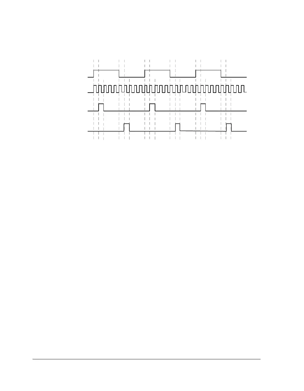
The second
INVFSA bit (bit 1) of the pulse width control register (PCG_PW)
determines whether the falling or rising edge is used. When set (= 1), this
bit selects an active low frame sync, and the pulse is generated during the
low period of clock input. When cleared (= 0), this bit is set to active high
frame sync and the pulse is generated during the high period of clock
input. For more information on the PCG_PWx registers, refer to Table A-66,
“PCG_PWx Register Bit Descriptions (in Bypass Mode),” on page A-159.
Programming Examples
This section contains three programming examples:
1. “PCG Setup for I2S or Left-Justified DAI” on page 13-15
2. “Clock and Frame Sync Divisors PCG Channel B” on page 13-20
3. “PCG Channel A and B Output Example” on page 13-23
Figure 13-5. One-Shot (Synchronous Clock Input and MISCA2_I)
CLOCK INPUT
FOR FRAME SYNC
MISCA2_I
FRAME SYNC OUTPUT
(INVFSA = 0, STROBEA = 1)
FRAME SYNC OUTPUT
(INVFSA = 1, STROBEA = 1)
 Loading...


