ADSP-21368 SHARC Processor Hardware Reference 3-61
External Port
Data Mask (DQM)
Since the ADSP-21367/8/9 and ADSP-2137x processors do not support
byte addressing, there is no need to mask data during partial writes (for
example, higher or lower byte on a 16-bit wide SDRAM).
L
All SDRAM DQM pins must be tied low.
SDC Configuration
After reset, the SDC clocks are enabled. However, the SDC must be con-
figured and initialized. Before programming the SDC and executing the
power-up sequence, select the correct CCLK to SDCLK ratio, and ensure that
the clock to the SDRAM is enabled (after the power has stabilized for the
proper amount of time as specified by the SDRAM).
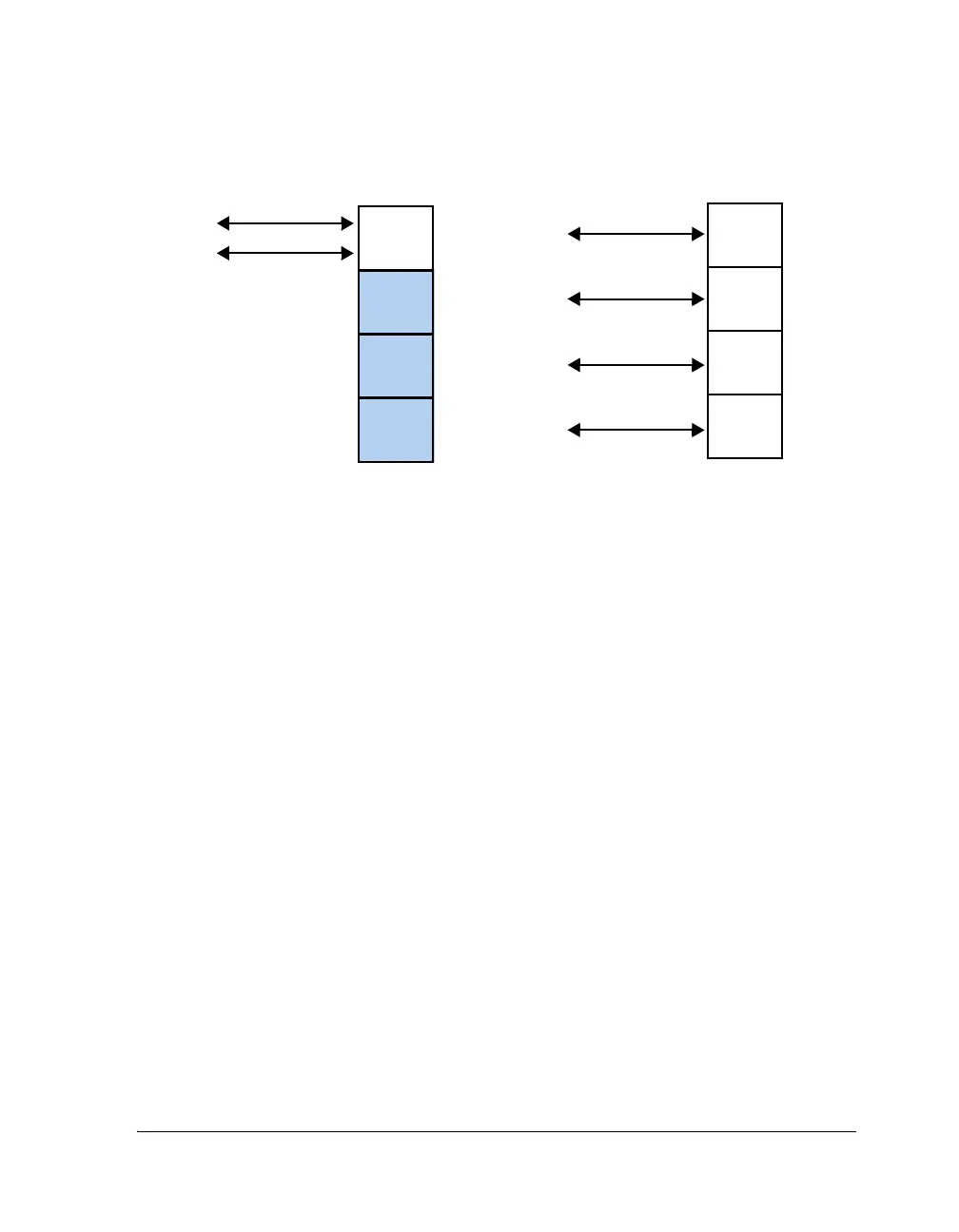
Figure 3-9. Single Versus Multibank Operation
Bank A
Bank B
Bank C
Bank D
Bank A
Bank B
Bank C
Bank D
Access to page x
Access to page y
Access to page x
Access to page y
Access to page x
Access to page y
Single bank operation Multibank operation
 Loading...


