Serial Peripheral Interface Registers
A-60 ADSP-21368 SHARC Processor Hardware Reference
SPI Baud Rate Registers (SPIBAUD, SPIBAUDB)
These registers’ addresses are 0x1005 (for SPIBAUD) and 0x2805 (for
SPIBAUDB) and their reset values are undefined (Table A-13). These SPI
registers are 16-bit, read-write registers that are used to set the bit transfer
rate for a master device. When configured as slaves, the value written to
these registers is ignored. The (SPIBAUDx) registers can be read or written
at any time. The serial clock rate is determined by the following formula:
SPI Baud Rate = (Peripheral clock rate (PCLK)) ÷ (4 × SPIBAUD15–1)
Writing a value of 0 or 1 to these registers disables the serial clock. There-
fore, the maximum serial clock rate is one-fourth the peripheral clock rate
(PCLK).
Various possible baud rate configurations are shown in Table A-14.
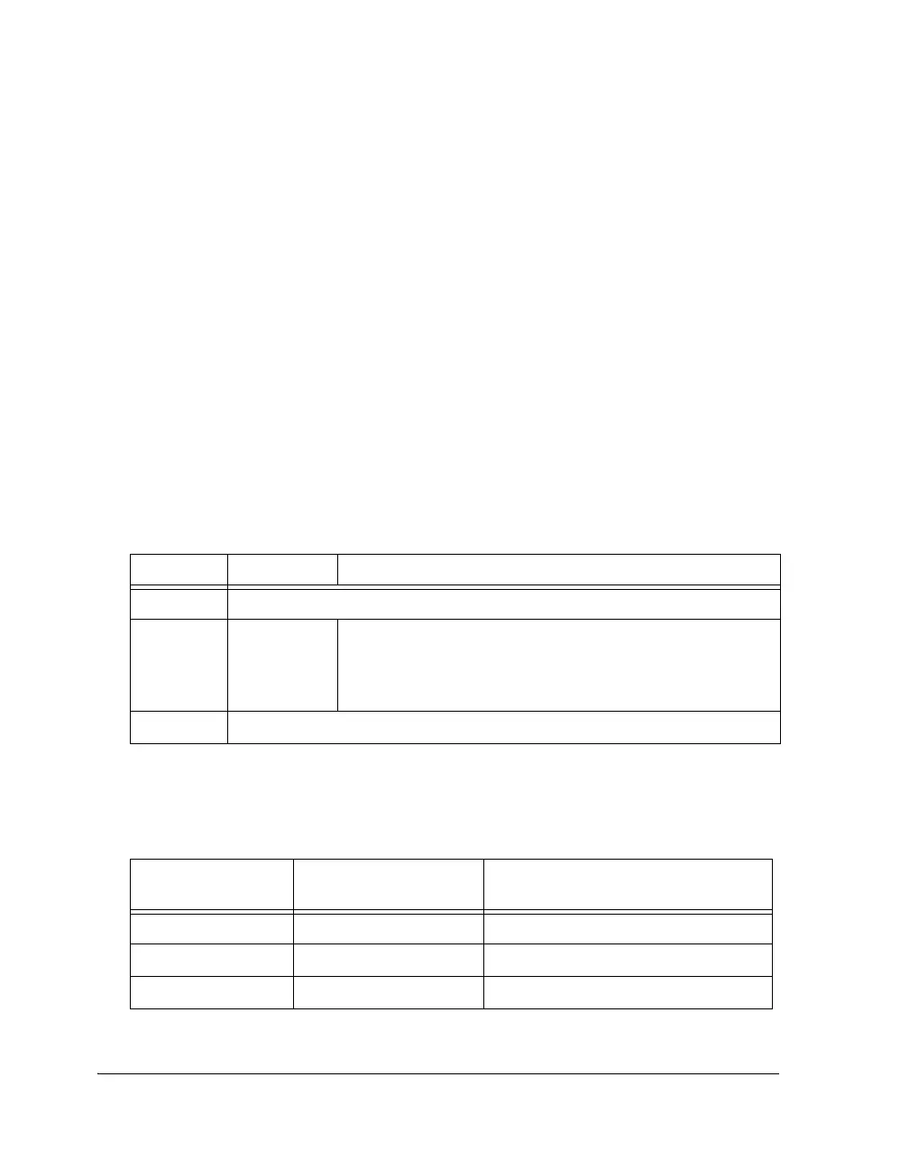
Table A-13. SPIBAUD, SPIBAUDB Register Bit Descriptions
Bit Name Description
0Reserved
15–1 BAUDR Baud Rate Enable. Enables the SPICLK per the following equa-
tion:
SPICLK baud rate = core clock (CCLK)/8 x BAUDR)
Default=0
31–16 Reserved
Table A-14. SPI Master Baud Rate Example
BAUDR
(Decimal Value)
SPI CLock Divide Factor Baud Rate for CCLK
0N/A N/A
18 41.7 MHz
2 16 20.8 MHz
 Loading...


