ADSP-21368 SHARC Processor Hardware Reference 3-67
External Port
Read/Write
This command is executed if the next read/write access is in the present
active page. During the read command, the SDRAM latches the column
address. The delay between activate and read commands is determined by
the t
RCD
parameter. Data is available from the SDRAM after the CAS
latency has been met.
In the write command, the SDRAM latches the column address. The
write data is also valid in the same cycle. The delay between activate and
write commands is determined by the t
RCD
parameter.
The SDC does not use the auto-precharge function of SDRAMs, which is
enabled by asserting SDA10 high during a read or write command.
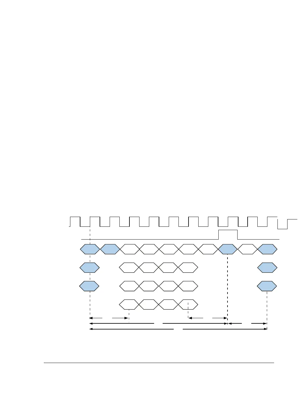
Figure 3-10 and Figure 3-11 show the SDRAM write and read timing of
the ADSP-21367/8/9 processors respectively. Figure 3-12 and
Figure 3-13 show the SDRAM write and read timing for the ADSP-2137x
processors.
Figure 3-10. Write Timing Diagram ADSP-21367/8/9
SDCLK
COMMAND
ACT
ACT
NOP
NO P
PREWR WR WR WR NOP
COL COL COL COL
AA AA
DDDD
ROW
A
ROW
A
t
RAS
t
RCD
t
RP
t
WR
t
RC
ADDR
BA[1:0]
DATA
SDA10
 Loading...


