ADSP-21368 SHARC Processor Hardware Reference 12-11
Two Wire Interface Controller
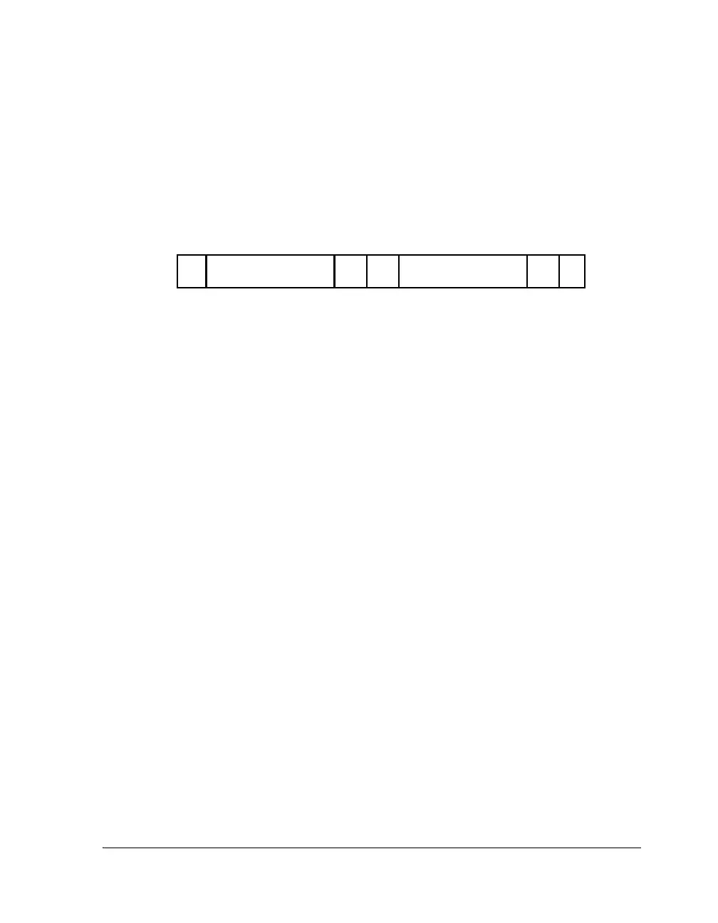
To better understand the mapping of TWI controller register contents to
a basic transfer, Figure 12-4 details the same transfer as above noting the
corresponding TWI controller bit names. In this illustration, the TWI
controller successfully transmits one byte of data. The slave has acknowl-
edged both address and data.
Clock Generation and Synchronization
The TWI controller only issues a clock during master mode operation and
only at the time a transfer has been initiated. If arbitration for the bus is
lost, the serial clock output immediately three-states. If multiple clocks
attempt to drive the serial clock line, the TWI controller synchronizes its
clock with the other remaining clocks. This is illustrated in Figure 12-5.
The TWI controller’s serial clock (SCL) output follows these rules:
• Once the clock high (
CLKHI) count is complete, the serial clock out-
put is driven low and the clock low (
CLKLOW) count begins.
• Once the clock low count is complete, the serial clock line is
three-stated and the clock synchronization logic enters into a delay
mode (shaded area) until the
SCL line is detected at a logic 1 level.
At this time, the clock high count begins.
Figure 12-4. Data Transfer With Bit Illustration
MADDR[6:0] MDIR ACK PACKS
S = START
P = STOP
ACK = ACKNOWLEDGE
TWI_XMT_BYTE
 Loading...


