Booting
14-42 ADSP-21368 SHARC Processor Hardware Reference
SPI Port Booting
The ADSP-21367/8/9 and ADSP-2137x processors support booting from
a host processor through the SPI slave (BOOT_CFG1–0 = 00), and booting
from an SPI flash, SPI PROM, or a host processor through SPI master
mode (BOOT_CFG1–0 = 01).
L
The SPI can also be configured to boot using the pins in the digital
peripheral interface. For more information, see “DPI/SRU2 Con-
nection Groups” on page 4-51.
Both SPI boot modes support booting from 8-, 16-, or 32-bit SPI devices.
In all SPI boot modes, the data word size in the shift register is hardwired
to 32 bits. Therefore, for 8- or 16-bit devices, data words are packed into
the shift register to generate 32-bit words least significant bit (LSB) first,
which are then shifted into internal memory. The relationship between
the 32-bit words received into the RXSPI register and the instructions that
need to be placed in internal memory is shown in Figure 14-11.
For more information about 32- and 48-bit internal memory addressing,
see the “Memory” chapter in the ADSP-2136x SHARC Processor Program-
ming Reference.
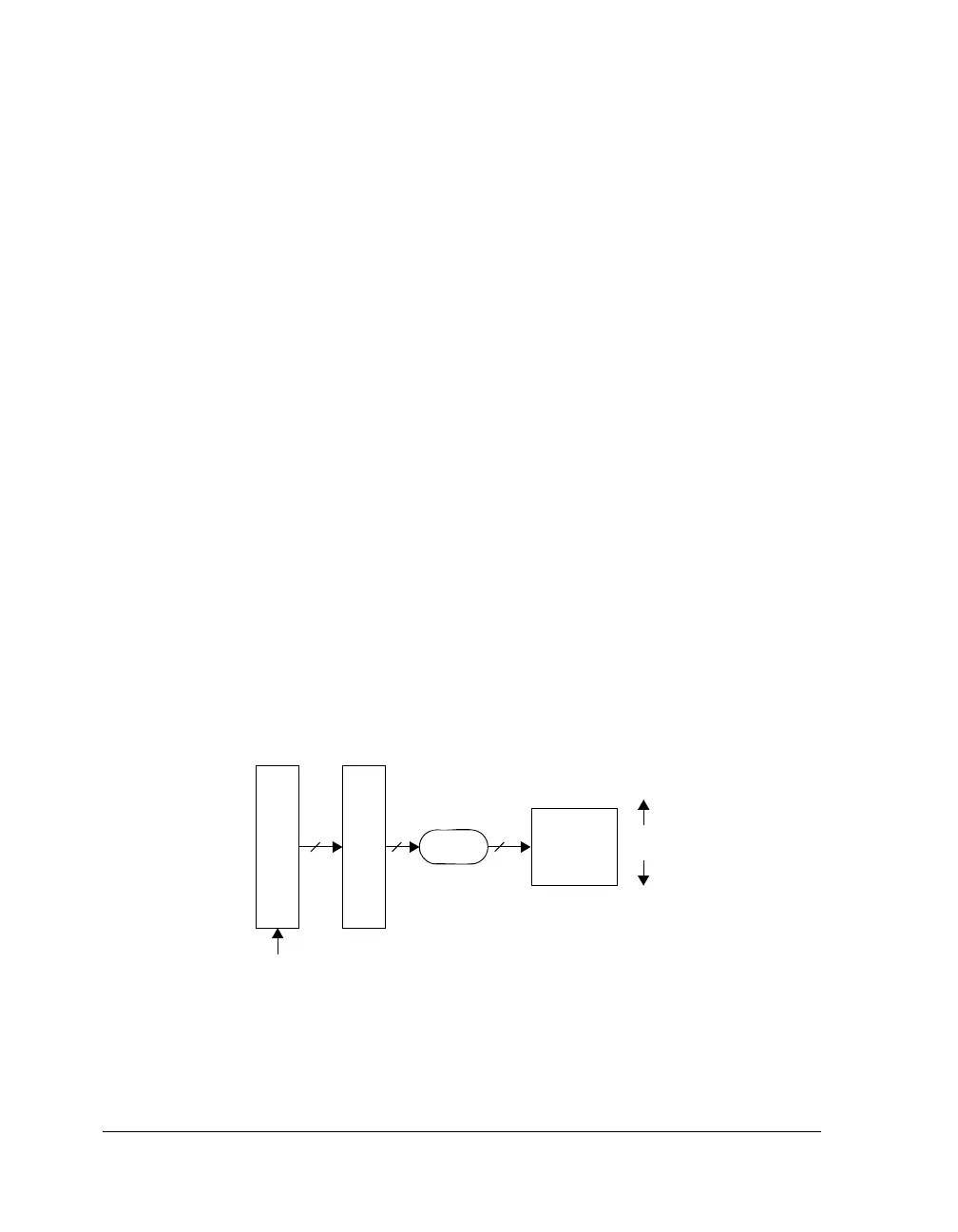
Figure 14-11. SPI Data Packing
MOSI
32-bit Receive
Shift Register
SPIRx
DMA
Internal
Memory
32 32
32
0x900FF
0x90000
256 48-bit
Words
 Loading...


