Precision Clock Generator Registers
A-158 ADSP-21368 SHARC Processor Hardware Reference
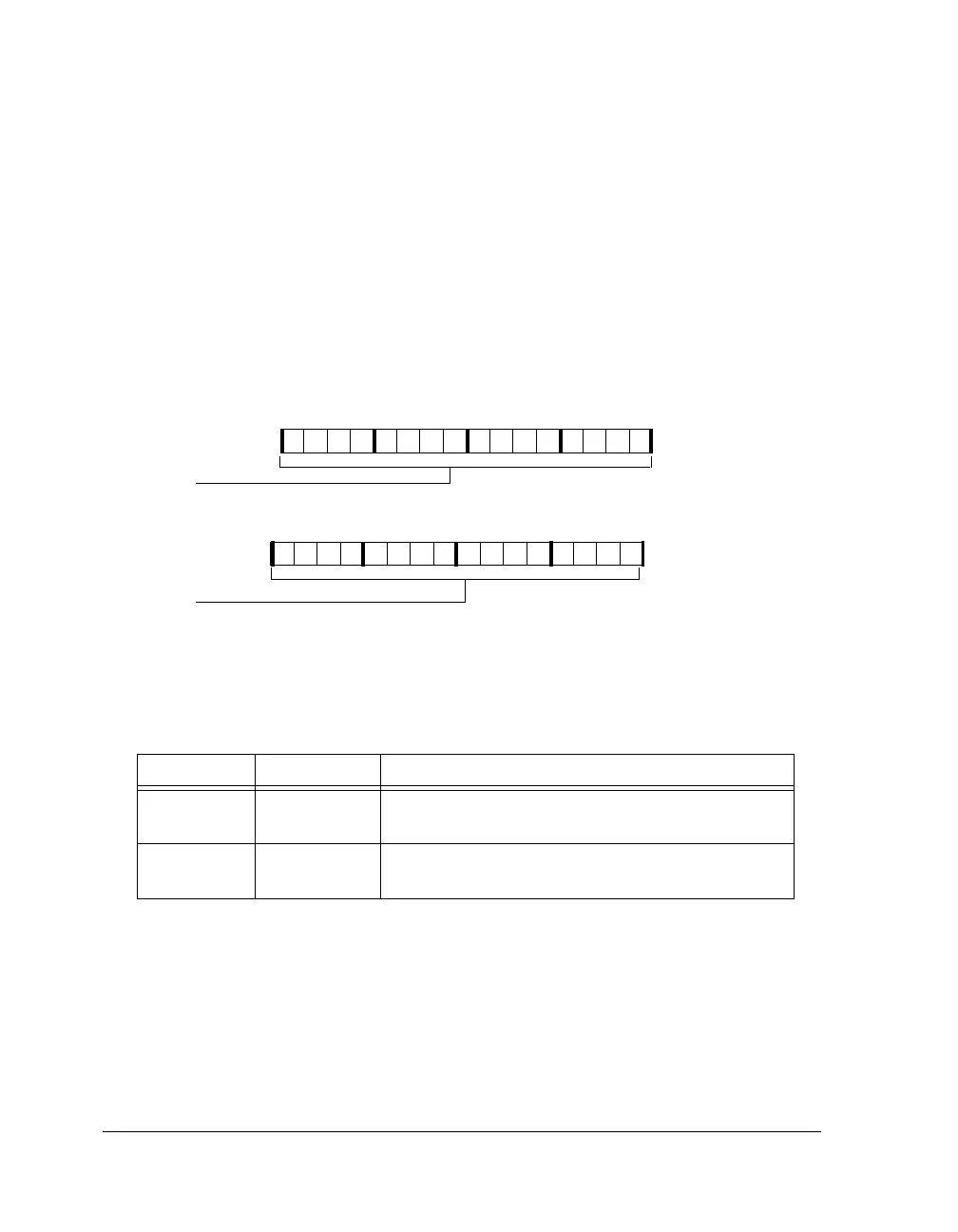
PCG Pulse Width Registers
Pulse width is the number of input clock periods for which the frame sync
output is HIGH. Pulse width should be less than the divisor of the frame
sync. The pulse width control registers are shown in Figure A-75 and
Figure A-76 and described in Table A-65 and Table A-66. Note that
where letters and slashes appear, for example A/B/C/D, any clock unit can
be chosen.
Figure A-75. PCG_PWx Registers (in Normal Mode)
Table A-65. PCG_PWx Register Bit Descriptions (in Normal Mode)
Bit Name Description
15–0 PWFSA Pulse Width for Frame Sync A/C.
Note: This is valid when not in bypass mode
31–16 PWFSB Pulse Width for Frame Sync B/D.
Note: This is valid when not in bypass mode
31 30 29 28 27 26 25 24 23 22 21 20 19 18 17 16
0000000000000000
15 14 13 12 11 10 9 8 7 6 5 4 3 2 1 0
0000000000000000
PWFSB
Pulse Width Frame Sync A/C
PWFSA
Pulse Width Frame Sync B/D
PCG_PW (0x24C4)
PCG_PW2 (0x24CA)
 Loading...


