ADSP-21368 SHARC Processor Hardware Reference A-133
Register Reference
Slave Mode Control Register (TWISCTL)
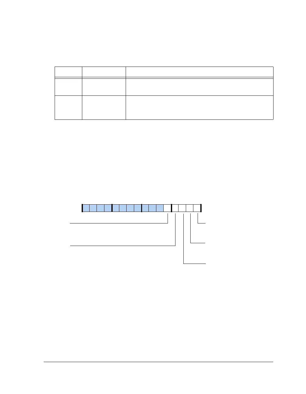
The TWI slave mode control register (TWISCTL) shown in Figure A-59 and
described in Table A-56, controls the logic associated with slave mode
operation. Settings in this register do not affect master mode operation
and should not be modified to control master mode functionality.
Table A-55. Clock Divider Register Bit Descriptions
Bit Name Description
7–0 CLKLOW Clock Low. Number of internal time reference periods the serial
clock (SCL) is held low. Represented as an 8-bit binary value.
15–8 CLKHI Clock High. Number of internal time reference periods the
serial clock (SCL) waits before a new clock low period begins
(assuming a single master). Represented as an 8-bit binary value.
Figure A-59. Slave Mode Control Register
15 14 13 12 11 10 9 8 7 6 5 4 3 2 1 0
0000000000000000
TWISCTL (0x4408)
TWISEN
TWIDVAL
TWINAK
TWIGCE
TWISLEN
Slave Enable
0=Slave not enabled
1=Slave enabled
Slave Address Length
0=Address is a 7-bit address
1=Reserved
Slave Transmit Data Valid
0=Data is for master mode
transmits only
1=Data is available for slave
mode transmits
Not Acknowledge
0=Slave RX transfer generates ACK at the conclu-
sion of a data transfer
1=Slave RX transfer generates a data NAK at the
conclusion of a data transfer
General Call Enable
0=General call address matching is not enabled
1=General call address matching is enabled
 Loading...


