ADSP-21368 SHARC Processor Hardware Reference 2-29
I/O Processor
Addressing
Figure 2-3 shows a block diagram of the I/O processor’s address generator
(DMA controller). Table 2-6 lists the parameter registers for each DMA
channel. The parameter registers are uninitialized following a processor
reset.
The I/O processor generates addresses for DMA channels much the same
way that the data address generators (DAGs) generate addresses for data
memory accesses. Each channel has a set of parameter registers including
an index register and modify register that the I/O processor uses to address
a data buffer in internal memory. The index register must be initialized
with a starting address for the data buffer. As part of the DMA operation,
the I/O processor outputs the address in the index register onto the pro-
cessor’s I/O address bus and applies the address to internal memory
during each DMA cycle—a clock cycle in which a DMA transfer is taking
place.
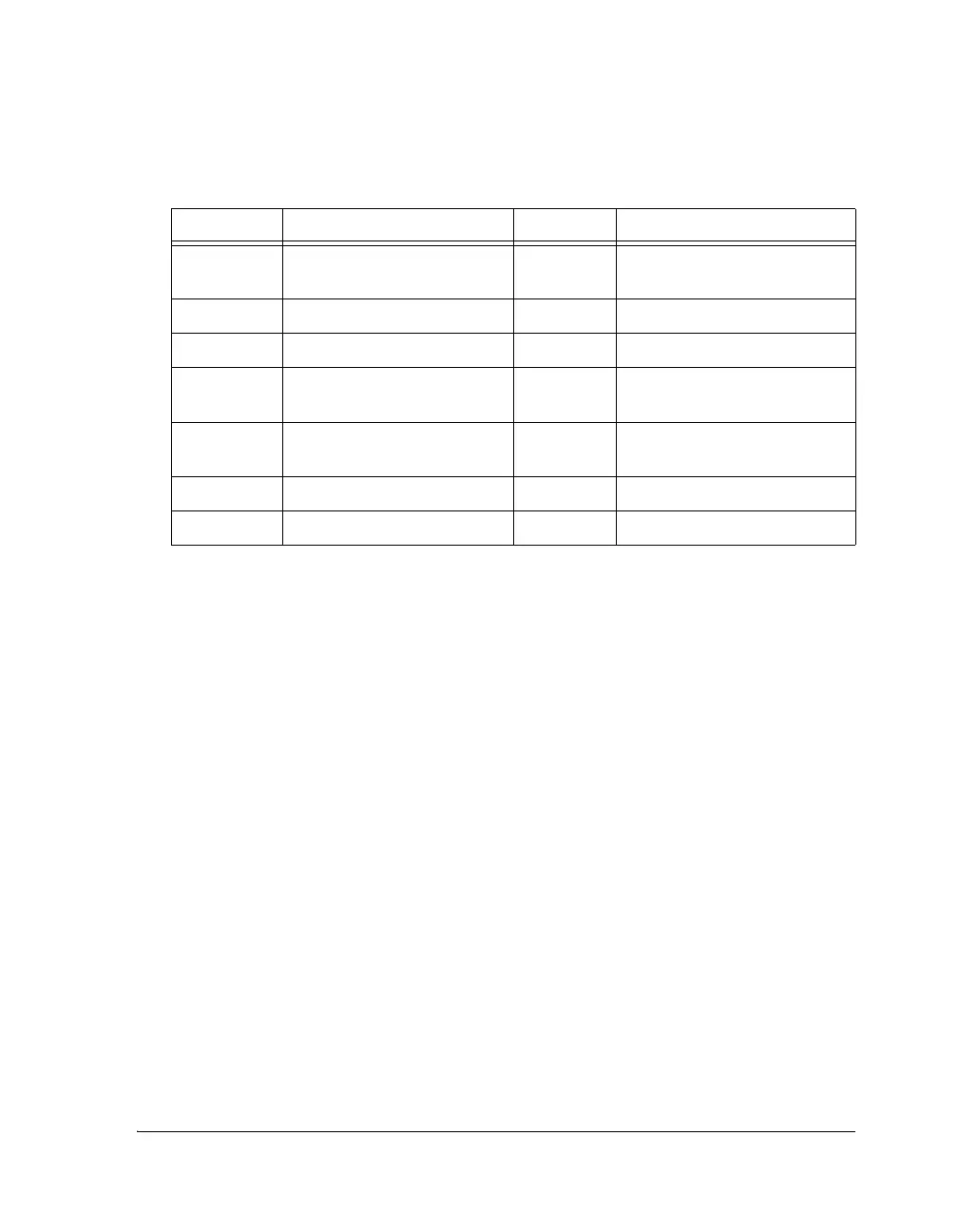
Table 2-6. DMA Parameter Registers
Register Function Width Description
IIy Internal Index Register 19 bits Address of buffer in internal
memory
IMxy Internal Modify Register 16 bits
1
Stride for internal buffer
Cxy Internal Count Register 16 bits Length of internal buffer
CPxy Chain Pointer Register 20 bits Chain pointer for DMA
chaining
EIEP External Index Register 19 bits Address of buffer in external
memory
EMEP External Modify Register 16 bits Stride for external buffer
ECEP External Count Register 16 bits Length of external buffer
1 IDP_DMA_Mx registers are 6 bits wide only.
 Loading...


