Signal Routing Units
4-12 ADSP-21368 SHARC Processor Hardware Reference
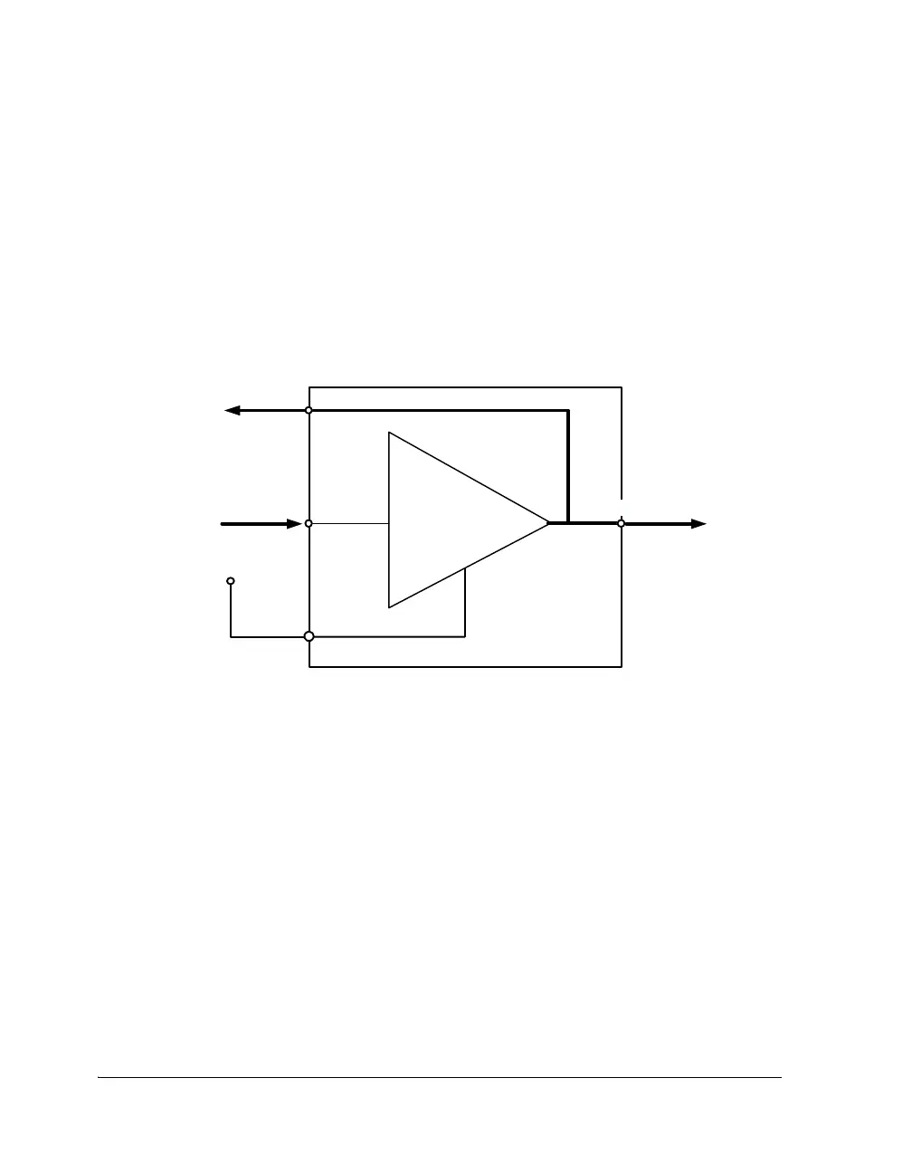
When the DAI/DPI pin is used only as an output, connect the corre-
sponding pin buffer enable to logic high as shown in Figure 4-7. This
enables the buffer amplifier to operate as a current source and to drive the
value present at the pin buffer input onto the DAI/DPI pin and off chip.
When the pin buffer enable (in this example
PBENxx_I) is set (= 1), the pin
buffer output (PBxx_O) is the same signal as the pin buffer input (PBxx_I),
and this signal is driven as an output.
Pin Buffers as Signal Input Pins
When the DAI/DPI pin is used only as an input, connect the correspond-
ing pin buffer enable to logic low as shown in Figure 4-8. This disables the
buffer amplifier and allows an off-chip source to drive the value present on
the DAI/DPI pin and at the pin buffer output. When the pin buffer
enable (
PBENxx_I) is cleared (= 0), the pin buffer output (PBxx_O) is the
signal driven onto the DAI pin by an external source, and the pin buffer
input (
PBxx_I) is not used.
Figure 4-7. Pin Buffer as Output
IN
OUT
PIN
ENABLE
DAI_PBxx_I
DAI_PBxx_O
PBENxx_I
EXTERNAL
PACKAGE
CONNECTION
PIN
INTERFACE
TO SRU
PAD
DRIVER
PIN BUFFER
OUTPUT
PIN BUFFER
INPUT
PIN BUFFER
ENABLE
(= HIGH)
DAI_PBxx_O
 Loading...


