ADSP-21368 SHARC Processor Hardware Reference 4-47
Digital Audio/Digital Peripheral Interfaces
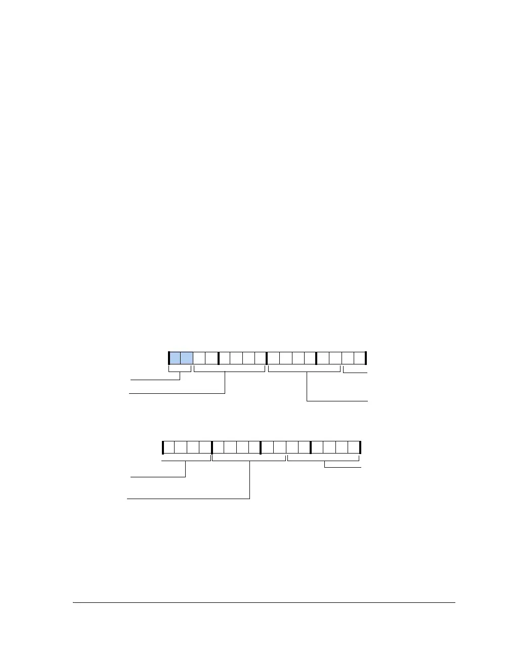
Group F—Pin Enable Signals
Group F signals, shown in Figure 4-37 through Figure 4-40 and described
in Table 4-9, are used to specify whether each DAI pin is used as an out-
put or an input by setting the source for the pin buffer enables. When a
pin buffer enable (
DAI_PBENxx_I) is set (= 1) the signal present at the cor-
responding pin buffer input (DAI_PBxx_I) is driven off chip as an output.
When a pin buffer enable is cleared (= 0) the signal present at the corre-
sponding pin buffer input is ignored.
The pin enable control registers activate the drive buffer for each of the 20
DAI pins. When the pins are not enabled (driven), they can be used as
inputs.
L
The following note applies to the group F connections.
SRU_PBEN0, SRU_PBEN1, SRU_PBEN2 and SRU_PBEN3 are 30 bit regis-
ters. On reads, bits 30 and 31 always return zero.
Figure 4-37. SRU_PBEN0
31 30 29 28 27 26 25 24 23 22 21 20 19 18 17 16
0000011100010010
Reserved
15 14 13 12 11 10 9 8 7 6 5 4 3 2 1 0
0100000101100101
DAI Port 5 Pin Buffer Enable Input
PBEN05_I
DAI Port 3 Pin Buffer Enable Input
PBEN03_I
DAI Port 1
Pin Buffer Enable Input
PBEN01_I
DAI Port 4
Pin Buffer Enable Input
PBEN04_I
DAI Port 2 Pin Buffer Enable Input
PBEN02_I
SRU_PBEN0 (0x2478)
PBEN03_I
DAI Port 3
Pin Buffer Enable Input
Reset = 0x0E2482CA
 Loading...


