Signal Routing Units
4-10 ADSP-21368 SHARC Processor Hardware Reference
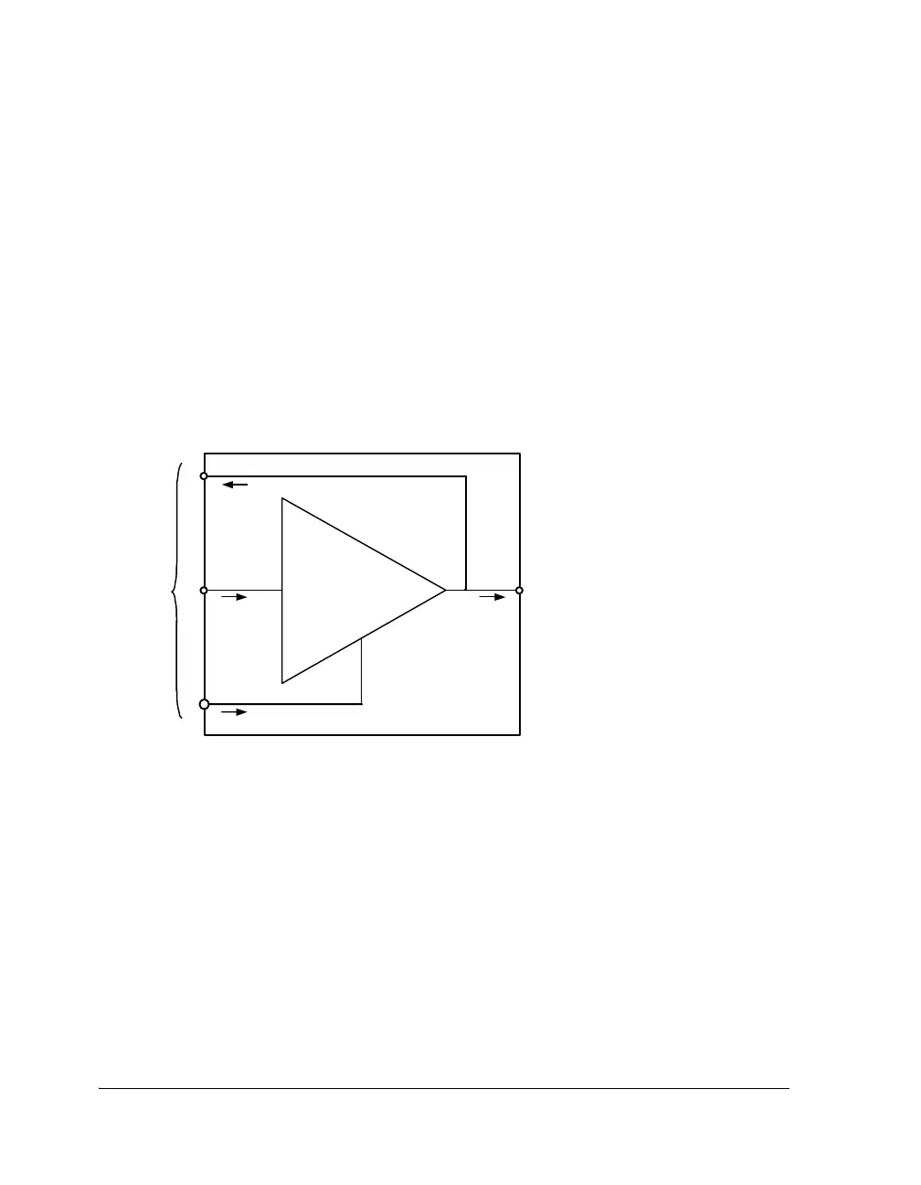
Pin Interface
Within the context of the SRUs, physical connections to the DAI/DPI
pins are replaced by a logical interface known as a pin buffer. This is a
three-terminal active device capable of sourcing/sinking output current
when its driver is enabled, and passing external input signals when dis-
abled. Each pin has an input, output, and enable pin as shown in
Figure 4-6. The inputs and the outputs are defined with respect to the
pin, similar to a peripheral device. This is consistent with the SRU nam-
ing convention.
The notation for pin input and output connections can be quite confusing
at first because, in a typical system, a pin is simply a wire that connects to
a device. The manner in which the pins are connected within the SRU
requires additional nomenclature. The pin interface’s input may be
thought of as the input to a buffer amplifier that can drive a load on the
physical external lead. The pin interface enable is the input signal that
enables the output of the buffer by turning it on when its value is logic
high, and turning it off when its value is logic low.
Figure 4-6. Pin Buffer Example
IN
OUT
ENABLE
PBxx_I
PBxx_O
PBENxx_I
External
Package
Connection
Pin
Interface
to SRU
PBxx_O
PIN
BUFFER
 Loading...


