Phase Shift
13-12 ADSP-21368 SHARC Processor Hardware Reference
Bypass Mode
When the divisor for the frame sync has a value of 0 or 1, the frame sync is
in bypass mode, and the PCG_PW and PCG_PW2 registers have different func-
tionality than in normal mode. Two bit fields determine the operation in
this mode. The one-shot (which is a strobe pulse) frame sync A, B, C, or
D (STROBEx) bit (bits 0 and 16 in the PCG_PW and PCG_PW2 registers, respec-
tively) determines if the frame sync has the same width as the input, or of
a single strobe. The active low frame sync select for the frame syncs
(INVFSx) bit (bits 1 and 17 of the PCG_PW and PCG_PW2 registers respec-
tively) determines the nature of the output in the simple bypass and single
strobe modes as described below. For additional information about the
PCG_PWx registers, see Figure A-76 on page A-159.
L
In bypass mode, bits 15–2 and bits 31–18 of the PCG_PWx registers
are ignored.
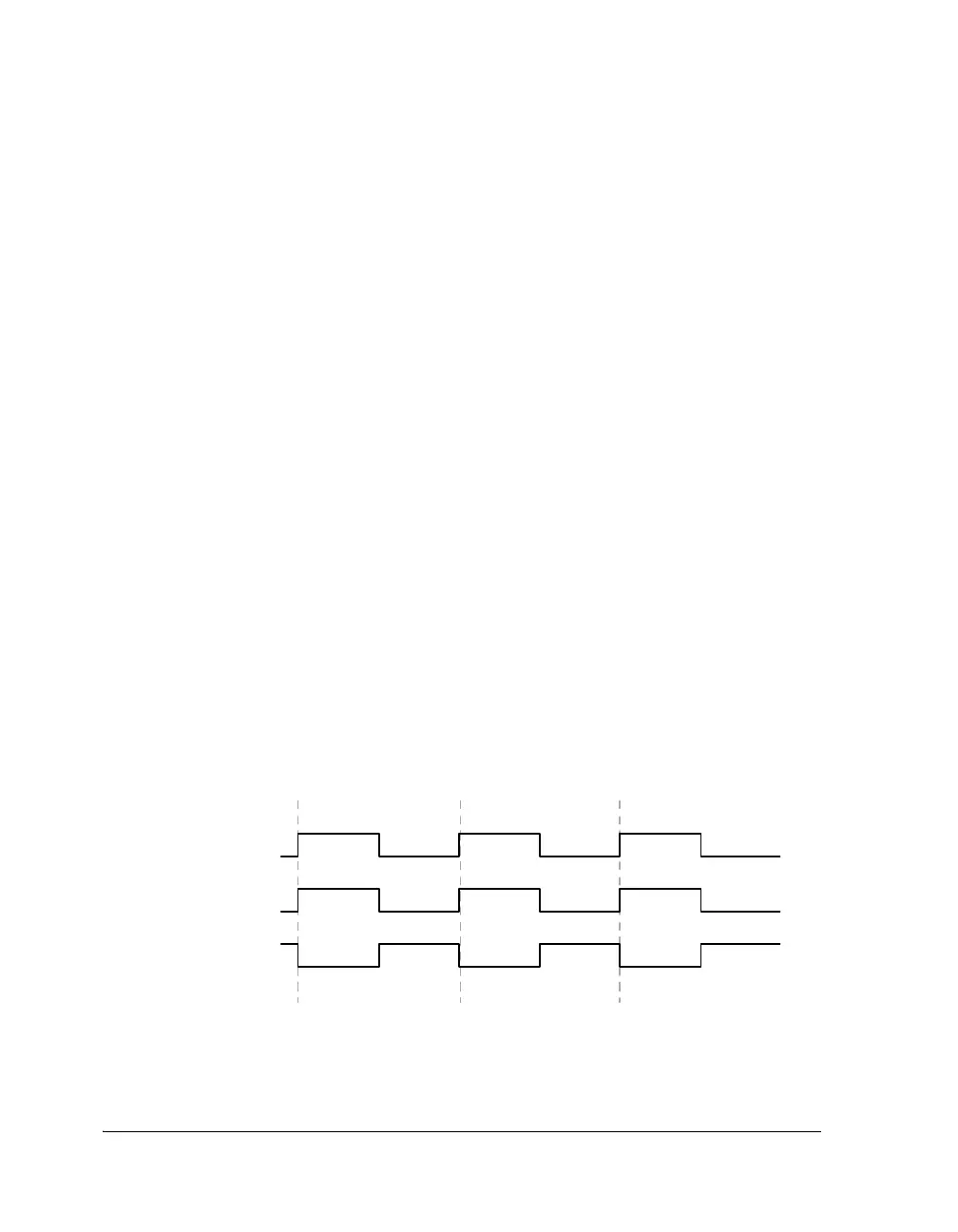
Bypass as a Pass Through
When the STROBEx bit in the PCG_PWx register equals 0, the unit is
bypassed and the output equals the input. If, for example, INVFSA (bit 1)
for unit A or INVFSB (bit 17) for unit B is set, then the signal is inverted
(see Figure 13-4).
Figure 13-4. Frame Sync Bypass
CLOCK INPUT
FOR FRAME SYNC
FRAME SYNC OUTPUT
(INVFSA = 0, STROBEA = 0)
FRAME SYNC OUTPUT
(INVFSA = 1, STROBEA = 0)
 Loading...


