ADSP-21368 SHARC Processor Hardware Reference A-159
Register Reference
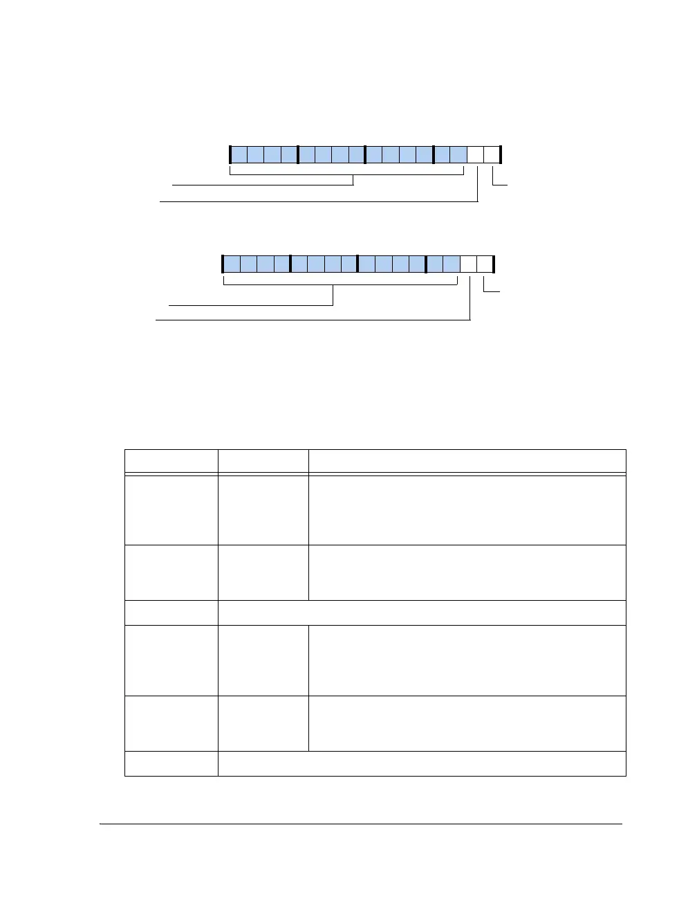
Figure A-76. PCG_PWx Registers (in Bypass Mode)
Table A-66. PCG_PWx Register Bit Descriptions
(in Bypass Mode)
Bit Name Description
0STROBExOne Shot Frame Sync A/C. Frame sync is a pulse with dura-
tion equal to one period of the MISCA2_I signal repeating at
the beginning of every frame.
Note: This is valid in bypass mode only.
1INVFSxActive Low Frame Sync Select for Frame Sync A/C.
0 = Active high frame sync
1 = Active low frame sync
15–2 Reserved (In bypass mode, bits 15-2 are ignored.)
16 STROBEx One Shot Frame Sync B/D. Frame sync is a pulse with dura-
tion equal to one period of the MISCA3_I signal repeating at
the beginning of every frame.
Note: This is valid in bypass mode only
17 INVFSx Active Low Frame Sync Select.
0 = Active high frame sync
1 = Active low frame sync
31–18 Reserved (In bypass mode, bits 31–18 are ignored.)
31 30 29 28 27 26 25 24 23 22 21 20 19 18 17 16
0000000000000000
Reserved
15 14 13 12 11 10 9 8 7 6 5 4 3 2 1 0
0000000000000000
One Shot Frame
Sync B/D
STROBEB
INVFSB
Active Low Frame Sync B/D
Reserved
One Shot Frame
Sync A/C
STROBEA
INVFSA
Active Low Frame Sync A/C
PCG_PW (0x24C4)
PCG_PW2 (0x24CA)
 Loading...


