ADSP-21368 SHARC Processor Hardware Reference A-155
Register Reference
Precision Clock Generator Registers
The precision clock generator (PCG) consists of four identical units. Each
of these units (A, B, C, and D) generates one clock (CLKA_O CLKB_O,
CLKC_O or CLKD_O) and one frame sync (FSA_O, FSB_O, FSC_O or FSD_O) out-
put. These units can take an input clock signal from a crystal oscillator
buffer output or any of the sources in Group A of the signal routing unit
(SRU).
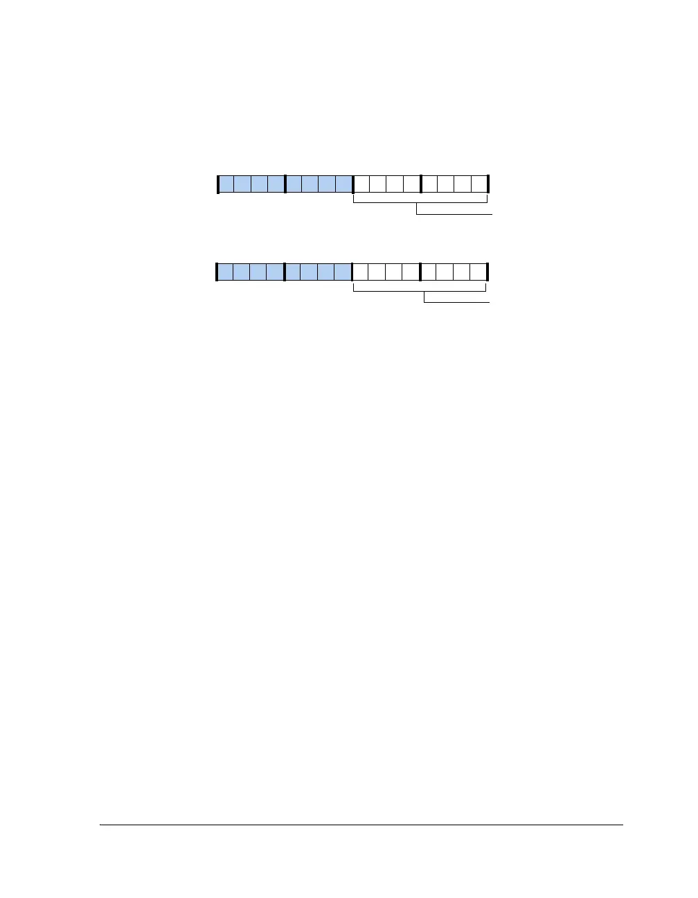
Control Registers (PCG_CTLxx)
The control registers operate exactly the same for each clock unit. The
control registers enable clocks, frame syncs, and select divisors for each
clock unit. These registers are shown in Figure A-73 and Figure A-74 and
described in Table A-63 and Table A-64. Note that where letters and
slashes appear, for example A/B/C/D, any clock unit can be chosen.
Figure A-72. 16-Bit Receive FIFO Register
15 14 13 12 11 10 9 8 7 6 5 4 3 2 1 0
0000000000000000
RCVDATA16[7:0]
RXTWI16 (0x4484)
31 30 29 28 27 26 25 24 23 22 21 20 19 18 17 16
0000000000000000
RCVDATA16[23:16]
Byte0
Byte1
 Loading...


