ADSP-21368 SHARC Processor Hardware Reference A-157
Register Reference
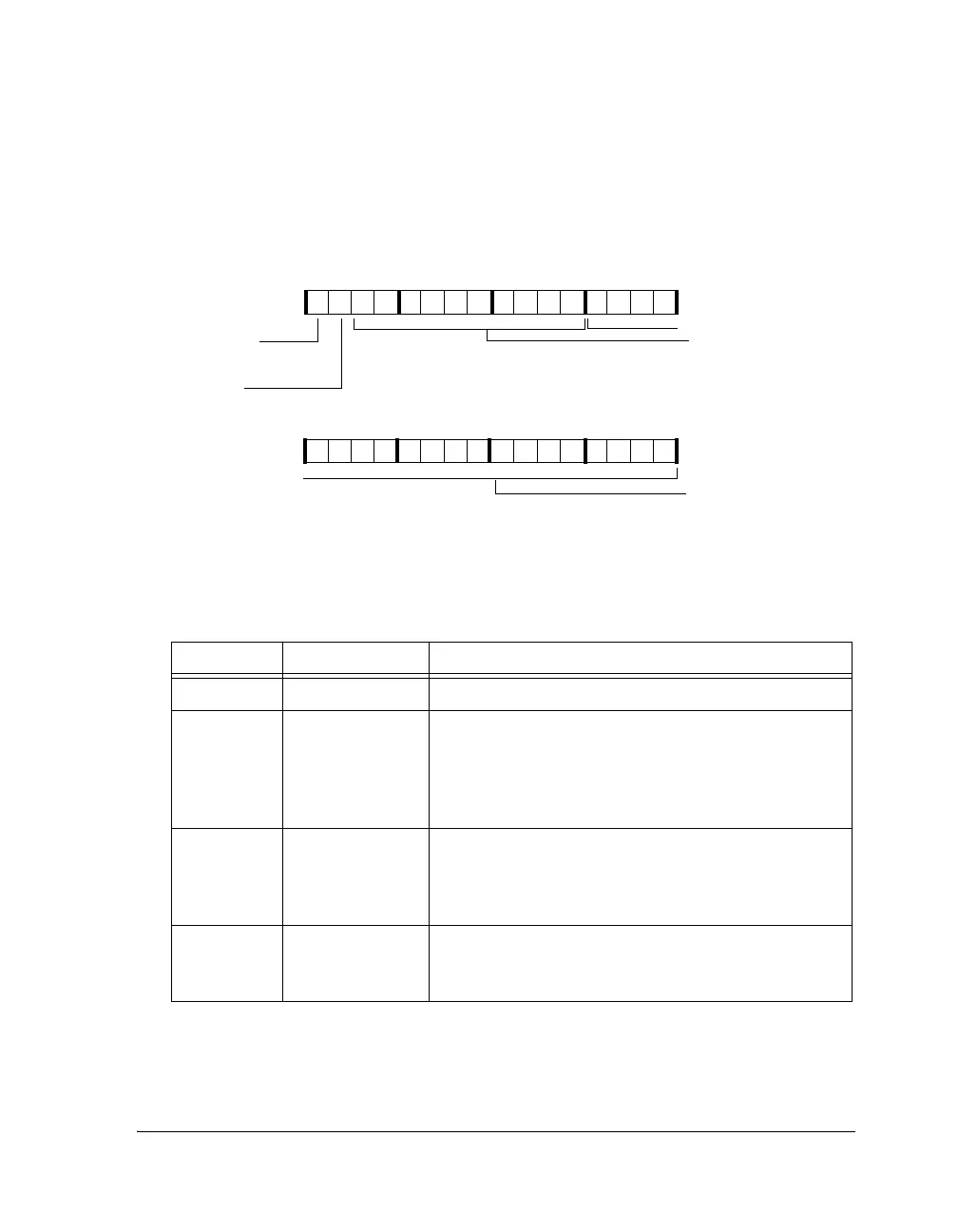
Figure A-74. PCG_CTLx1 Register
Table A-64. PCG_CTLx1 Register Bit Descriptions
Bit Name Description
19–0 CLKxDIV Divisor for Clock A/B/C/D.
29–20 FSxPHASE_LO Phase for Frame Sync A/B/C/D.
This field represents the lower half of the 20-bit value for
the channel A/B/C/D frame sync phase. See also
FSXPHASE_HI (Bits 29-20) in PCG_CTLx1 described on
page A-156.
30 FSxSOURCE Frame Sync Source. Master clock source for frame sync
A/B/C/D.
0 = XTAL buffer output selected for specified frame sync
1 = PCG_EXTX_I selected for specified frame sync
31 CLKxSOURCE Clock Source. Master clock source for clock A/B/C/D.
0 = XTAL buffer output selected for specified clock
1 = PCG_EXTx_I selected for specified clock
31 30 29 28 27 26 25 24 23 22 21 20 19 18 17 16
0000000000000000
CLKXSOURCE
15 14 13 12 11 10 9 8 7 6 5 4 3 2 1 0
0000000000000000
Clock A/B/C/D Source
CLK A/B/C/D Divisor
CLKXDIV
Frame Sync
A/B/C/D Phase 9:0
FSXPHASE_LO
FSXSOURCE
Frame Sync A/B/C/D Source
PCG_CTLA1 (0x24C1)
PCG_CTLB1 (0x24C3)
PCG_CTLC1 (0x24C7)
PCG_CTLD1 (0x24C9)
 Loading...


