ADSP-21368 SHARC Processor Hardware Reference 14-25
System Design
2. The ADSP-2137x processor receives the command and completes
any unfinished work which may also include writing to the
RUN-
RSTCTL
register.
3. When the ADSP-2137x processor is ready to accept the running
reset, it signals the host over the command interface.
4. The host drives the running reset input into the ADSP-21375/71
processor.
Running Reset Control Register (RUNRSTCTL)
To program the running reset feature, (by toggling the RESETOUT pin), a
new register, running reset control (RUNRSTCTL) has been added to the
ADSP-2137x processor architecture.
This register is located at memory-mapped address 0x2100. On previous
generations of SHARCs, the RESETOUT/CLKOUT pin was an output. On the
ADSP-2137x processors, this pin is an input/output, and the sense and
direction of the pin is controlled by bit 0 of the RUNRSTCTL register (see
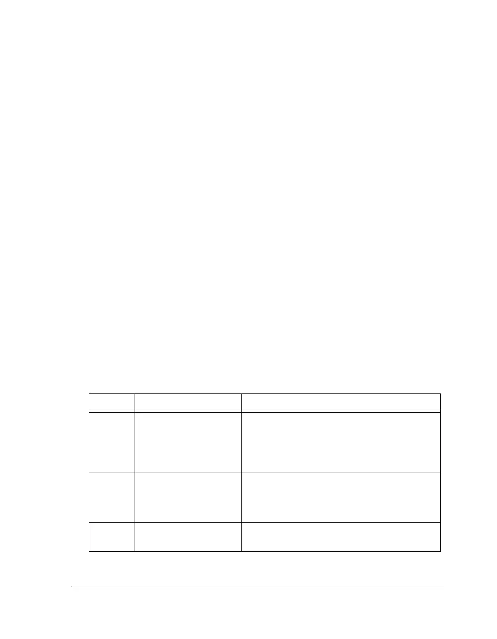
Table 14-4).
Table 14-4. Running Reset Control Register Bit Descriptions
Bit Name Description
0 PM_RUNRST_PINEN Configures the RESETOUT pin for RUNRST input.
Read Write
0 = RESETOUT pin is CLKOUT/RESETOUT
1 = RESETOUT pin is RUNRST input
Reset value = 0
1 PM_RUNRST_EN Enable the running reset functionality.
0 = Running reset disabled
1 = Running reset enabled
Reset value = 0
31–2 Reserved Reads return 0
Reset value = 0
 Loading...


