ADSP-21368 SHARC Processor Hardware Reference 3-21
External Port
AMI Timing Control
The following three sections introduce the available control settings that
affect the timing used to make AMI accesses. Note that all accesses are in
terms of SDCLK since the SDRAM controller and AMI share this clock.
Wait States
Wait states and acknowledge signals are used to allow the processors to
connect to memory-mapped peripherals and slower memories. Wait states
are programmable from 1 to 31 using the
WS bits (bits 10–6) in the AMI
control register. Wait states are programmed relative to
SDCLK.
When
ACK is enabled, the wait state value should be set to indicate when
the processor can sample ACK after the RD/WR edge goes low. The minimum
wait state value that can be used is
WS = 1 when ACK is enabled. If ACK is not
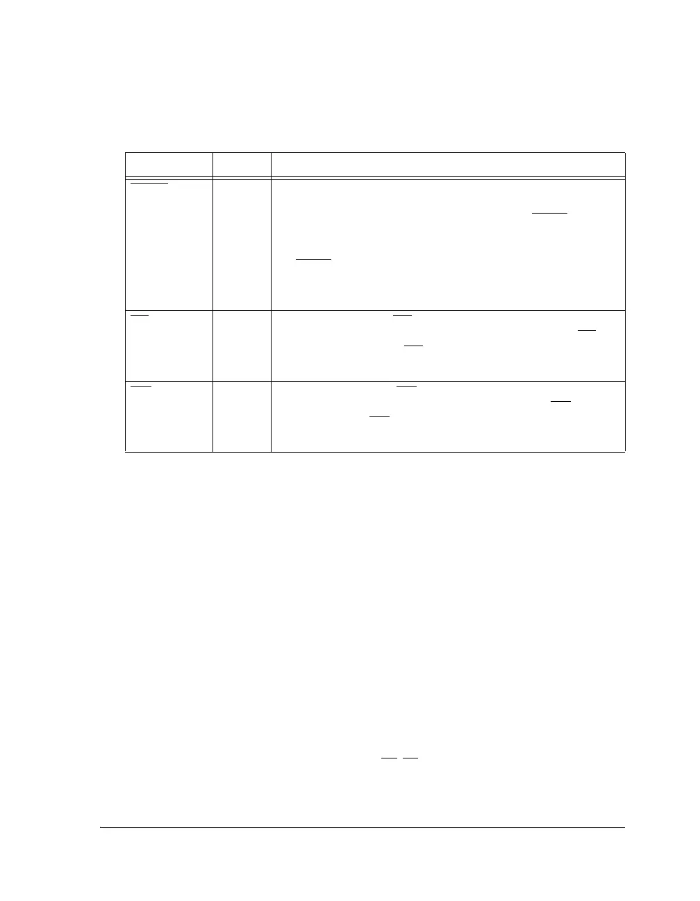
MS3–0 O Memory Select Lines [FLAG2-3 are muxed and used as MS2 and
MS3]. Memory select lines 0–1 are asserted (low) as chip selects for
the corresponding banks of external memory. The MS3-0 lines are
decoded memory address lines that change at the same time as the
other address lines. When no external memory access is occurring,
the MS3-0
lines are inactive; they are active however when a condi-
tional memory access instruction is executed, whether or not the
condition is true.
RD
O Memory Read Strobe. RD is asserted whenever the processor reads
a word from external memory. In a shared memory system, RD is
driven by the bus master. RD
has a 22.5 kΩ internal pull-up resistor
that is enabled for processors with ID2-0=01x during reset.
WR O Memory Write Strobe. WR is asserted when the processor writes a
word to external memory. In a shared memory system, WR is driven
by the bus master. WR
has a 22.5 kΩ internal pull-up resistor that is
enabled for processors with ID2-0=01x during reset.
Table 3-9. Asynchronous Memory Interface Signals (Cont’d)
Pin Type Description
 Loading...


