ADSP-21368 SHARC Processor Hardware Reference A-97
Register Reference
Sample Rate Converter Registers
The sample rate converter (SRC) is composed of five registers which are
described in the following sections.
SRC Control Registers (SRCCTLx)
These registers (read/write) control the operating modes, filters, and data
formats used in the SRCs and are shown in Figure A-36 through
Figure A-39 and described in Table A-42 and Table A-43. The SRCCTL0
register controls the SRC0 and SRC1 modules and SRCCTL1 register con-
trols the SRC2 and SRC3 modules.
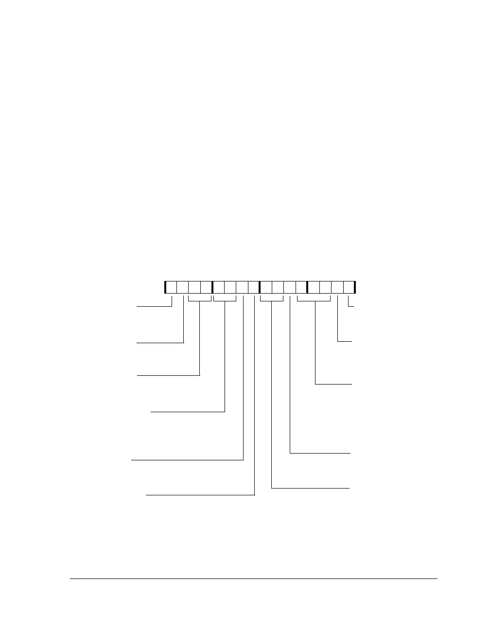
Figure A-36. SRCCTL0 Register (Bits 16–31)
31 30 29 28 27 26 25 24 23 22 21 20 19 18 17 16
0000000000000000
SRCCTL0 (0x2490)
SRC1_ENABLE
SRC1 Enable
1=SRC enabled
0=SRC disabled
SRC1_MPHASE
SRC1 Matched- Phase Mode
1=Enabled
0=Disabled
SRC1_LENOUT
SRC1 Output Word Length
00=24-bit, 01=20-bit
10=18-bit, 11=16-bit
SRC1_SMODEOUT
SRC1 Serial Output Format
00=Left-justified (default)
01=I
2
S
10=TDM Mode
11=Right-justified
SRC1_DITHER
SRC1 Dither Enable
1=Enable
0=Disable
SRC1 Soft Mute Enable
1=Mute (default)
0=No mute
SRC1_SOFTMUTE
SRC1_HARD_MUTE
SRC1 Hard Mute Enable
1=Enabled
0=Disabled
SRC1_AUTO_MUTE
SRC1 Auto Hard Mute
Enable (from SPDIF RX)
1=Enabled
0=Disabled
SRC1_BYPASS
SRC1 De-emphasis Filter
1=Enabled
0=Disabled (default)
SRC1 Bypass Mode
1=Bypass enabled
0=Bypass disabled
SRC1_DEEMPHASIS
SRC1_SMODEIN
SRC1 Serial Input Format
000=Left-justified (Default)
001=I
2
S
010=TDM
100=24-bit right-justified
101=20-bit right-justified
110=18-bit right-justified
111=16-bit right-justified
 Loading...


