Making Connections in the SRUs
4-36 ADSP-21368 SHARC Processor Hardware Reference
Group D Connections—Pin Signal Assignments
Group D is used to specify any signals that are driven off chip by the pin
buffers. A pin buffer input (
DAI_PBxx_I) is driven as an output from the
processor when the pin buffer enable is set (= 1).
Each physical pin (connected to a bonded pad) may be routed via the SRU
to any of the outputs of the DAI audio peripherals, based on the 7-bit val-
ues listed in Table 4-7 on page 4-39. The SRU may also be used to route
signals that control the pins in other ways. These signals may be config-
ured for use as general-purpose I/O, precision clock generators, or
miscellaneous control signals. The registers are shown in Figure 4-30
through Figure 4-34.
L
The following notes apply to the group D sources.
1. Setting
SRU_PIN4[28] to high inverts the level of DAI_P19_I
and setting SRU_PIN4[29] inverts the level of DAI_P20_I.
2. If
SRU_PIN4[20:14] = 0x12 then setting SRU_PIN4[28] to
high does not invert the output.
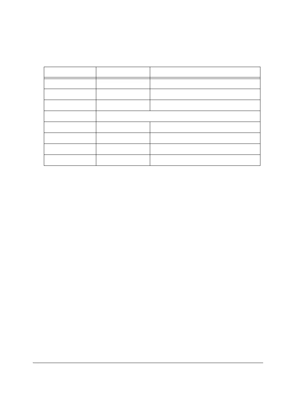
11000 (0x18) SPORT4_FS_O Select SPORT 4 frame sync
11001 (0x19) SPORT5_FS_O Select SPORT 5 frame sync
11010 (0x1A) DIR_FS_O SPDIF_RX frame sync output
11011 (0x1B) Reserved
11100 (0x1C) PCG_FSA_O Select precision frame sync A output
11101 (0x1D) PCG_FSB_O Select precision frame sync B output
11110 (0x1E) LOW Select logic level low (0)
11111 (0x1F) HIGH Select logic level high (1)
Table 4-6. Group C Sources—Frame Sync (Cont’d)
Selection Code Source Signal Description (Source)
 Loading...


