ADSP-21368 SHARC Processor Hardware Reference 3-49
External Port
SDRAM Control Status Register (SDSTAT)
The SDRAM control status register provides information on the state of
the SDC. This information can be used to determine when it is safe to
alter SDC control parameters, or as a debug aid. The status bits that
appear in this register are described in detail in “SDRAM Control Status
Register (SDSTAT)” on page A-26.
SDRAM Refresh Rate Control Register (SDRRC)
The SDRAM refresh rate control register provides a flexible mechanism
for specifying auto-refresh timing. The SDC provides a programmable
refresh counter which has a period based on the value programmed into
the lower 12 bits of this register. This coordinates the supplied clock rate
with the SDRAM device’s required refresh rate.
The delay (in number of
SDCLK cycles) between consecutive refresh
counter time-outs must be written to the
RDIV field. A refresh counter
time-out triggers an auto-refresh command to the external SDRAM bank.
Programs should write the
RDIV value to the SDRRC register before the
SDRAM power-up sequence is triggered. Change this value only when the
SDC is idle as indicated in the SDSTAT register.
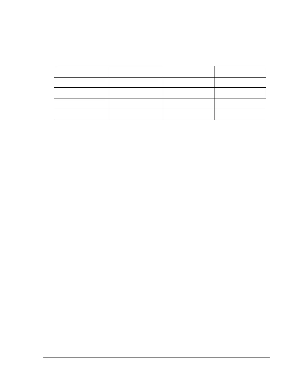
Table 3-19. SDRAM Row Address Width Bit Settings
SDRAW Bit Setting Row Address Width SDRAW Bit Setting Row Address Width
SDRAW8 = 000 8 bits (256) SDRAW12 = 100 12 bits (4K)
SDRAW9 = 001 9 bits (512) SDRAW13 = 101 13 bits (8K)
SDRAW10 = 010 10 bits (1K) SDRAW14 = 110 14 bits (16K)
SDRAW11 = 011 11 bits (2K) SDRAW15 = 111 15 bits (32K)
 Loading...


