SDRAM Controller
3-48 ADSP-21368 SHARC Processor Hardware Reference
For more information, see “Timing External Memory Accesses” on
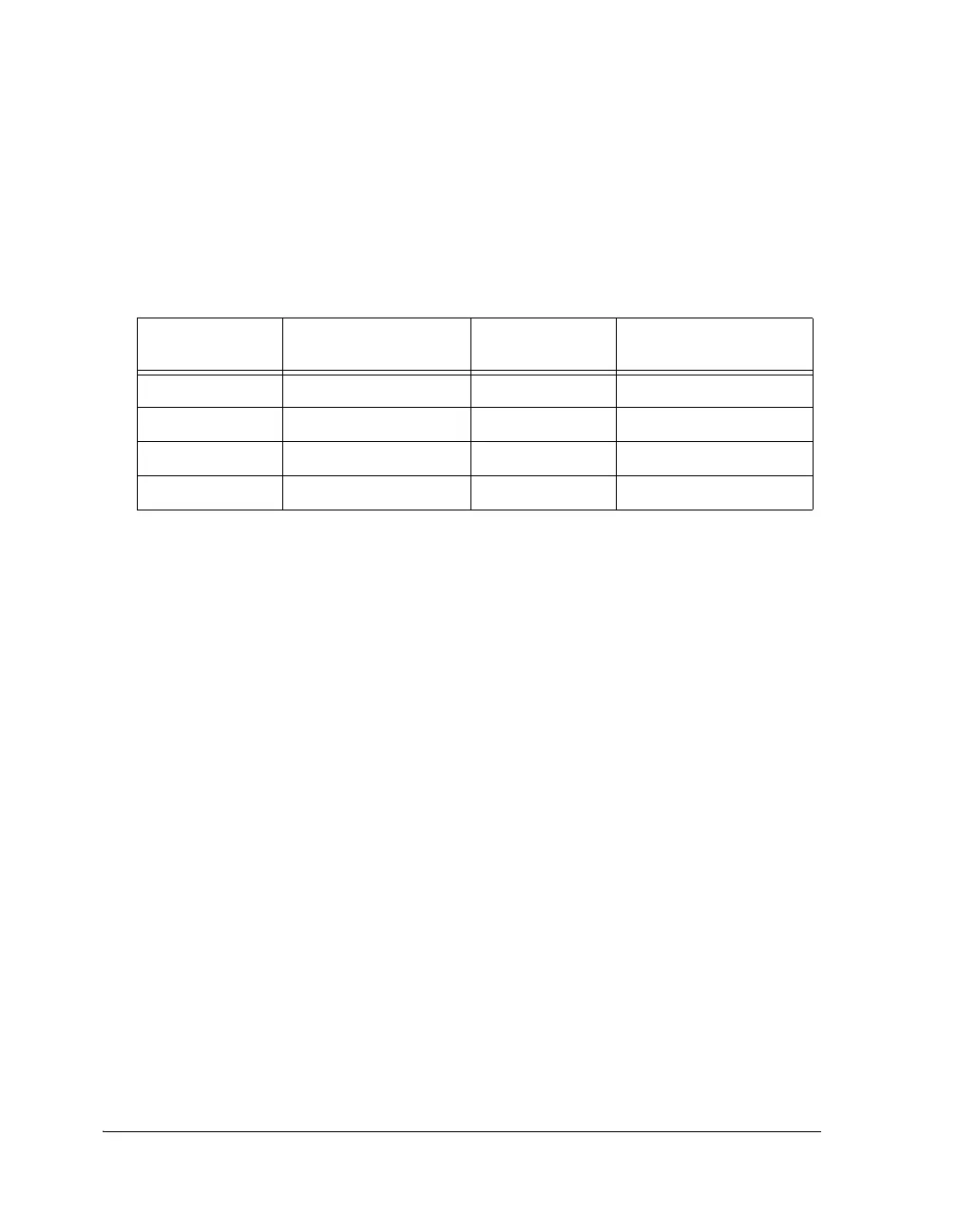
page 3-36. Any value between 1 and 7
SDCLK cycles may be selected as
shown in Table 3-18.
SDRAM row address width. SDRAW bits 29–27. With the X16DE and SDCAW
bits, defines the SDRAM core memory space (internal address to external
address mapping). Any value between 0 to 7 can be selected as shown in
Table 3-19. For more information, see “SDRAM Address Mapping” on
page 3-51.
Program the SDRAM Controller for Page Size of 128 Words. PGSZ 128
bit 30. This bit allows programs to configure the SDC for a page size of
128 words (7 bits) which supports most available 32 Mb SDRAMs.
No burst mode.
NO BSTOP bit 31. This bit is used to select between full
page burst or no burst mode (BL=1). If set (=1), no burst mode is active
and the burst stop command is ignored. If cleared, full page burst is active
using the burst stop command for access interruption. This bit must be
cleared if the SDRAM does not support no burst mode but supports full
page burst.
Table 3-18. SDRAM t
RCD
Bit Settings
SDTRCD Bit
Setting
SDRAM Parameter
Setting
SDTWR Bit
Setting
SDRAM Parameter
Setting
000 Reserved STDRCD4 = 100 Four clock cycles
STDRCD1 = 001 One clock cycle STDRCD5 = 101 Five clock cycles
STDRCD2 = 010 Two clock cycles STDRCD6 = 110 Six clock cycles
STDRCD3 = 011 Three clock cycles STDRCD7 = 111 Seven clock cycles
 Loading...


