UART Control and Status Registers
11-6 ADSP-21368 SHARC Processor Hardware Reference
A sampling clock equal to 16 times the baud rate samples the data as close
to the midpoint of the bit as possible. Because the internal sample clock
may not exactly match the asynchronous receive data rate, the sampling
point drifts from the center of each bit. The sampling point is synchro-
nized again with each start bit, so the error accumulates only over the
length of a single word. A receive filter removes spurious pulses of less
than two times the sampling clock period.
The 32-bit, read-only
UARTxRBR register is mapped to the same address as
the write-only UARTxTHR and UARTxDLL registers. In no pack mode
(default), only the lower byte is used—all other bits are zero-filled. How-
ever in pack mode, both the high and low bytes are used. The RX9Dx bits
are the 9th bit in 9-bit transmission mode. To access UARTxRBR, the UARTD-
LAB bit in the UARTxLCR register must be cleared. When the UARTDLAB bit is
cleared, writes to this address target the UARTxTHR register, while reads
from this address return the UARTxRBR register.
L
Because of the destructive nature of reading these registers, shadow
registers are provided for reading the contents of the corresponding
main registers. The shadow registers,
UARTxRBRSH, return exactly
the same contents as the main register, but without changing the
status in any way. These registers are 32-bit registers located at
address 0x3C08 (for UART0RBRSH) and 0x4008 (for UART1RBRSH).
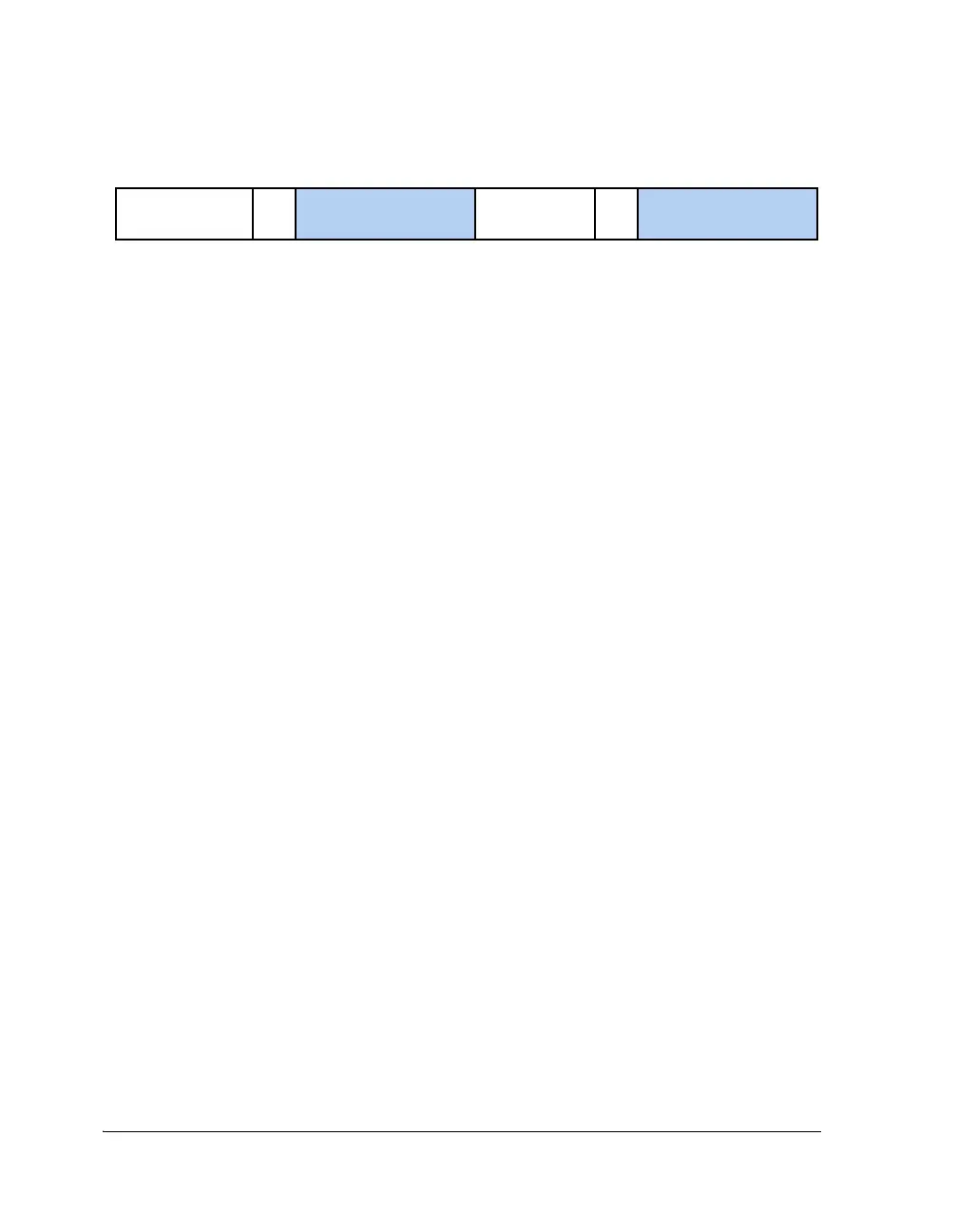
Figure 11-3. Receive Buffer Register (Packing Enabled)
31 0781524 23
RX9D0
9
RX9D1 ZERO-FILLED
LOWER BYTE
HIGHER BYTEZERO-FILLED
 Loading...


