ADSP-21368 SHARC Processor Hardware Reference 12-3
Two Wire Interface Controller
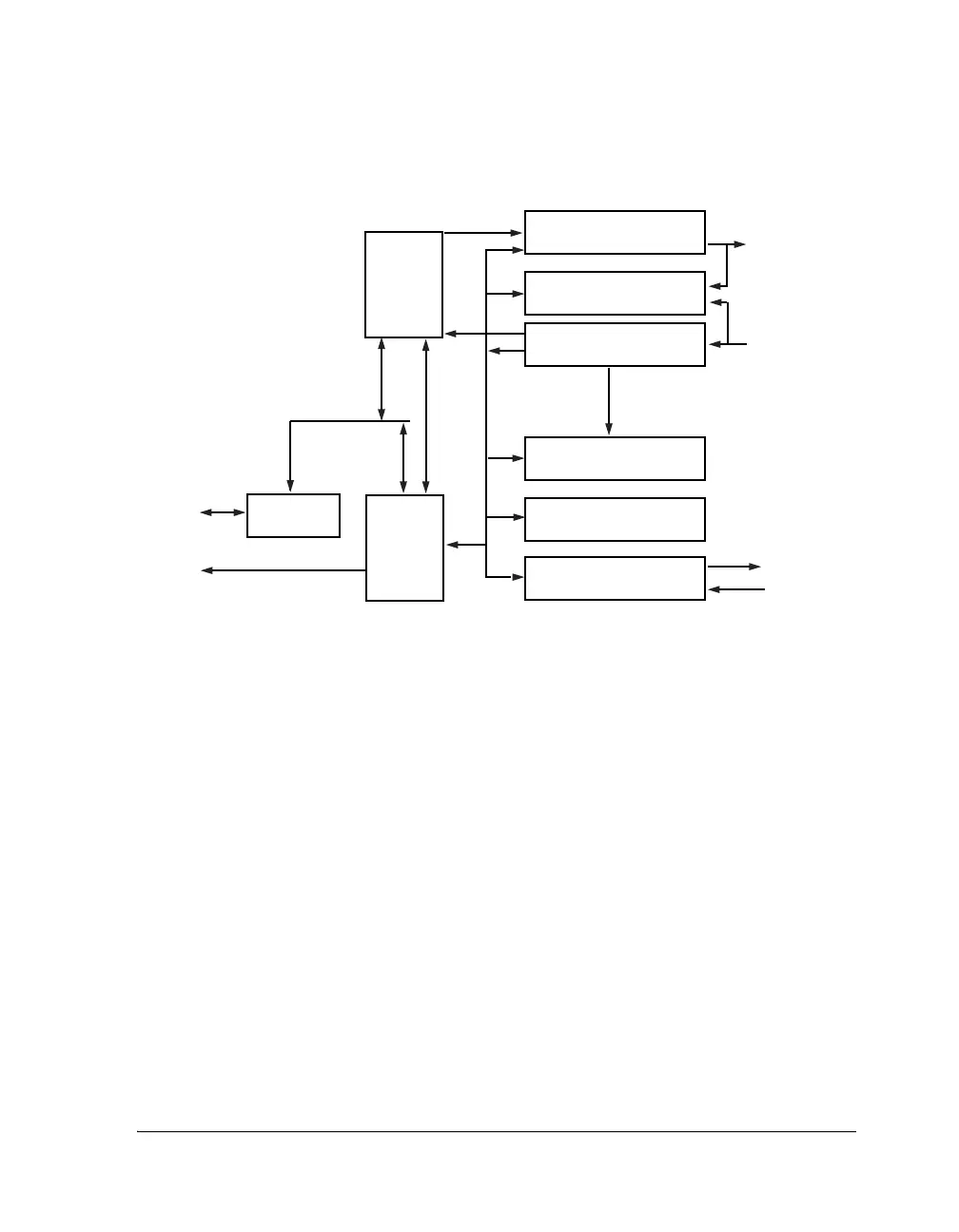
The transmit shift register serially shifts its data out externally off chip.
The output can be controlled to generate acknowledgements or it can be
manually overwritten.
The receive shift register receives its data serially from off chip. The
receive shift register is 1 byte wide and data received can either be trans-
ferred to the FIFO buffer or used in an address comparison.
The address compare block supports address comparison in the event the
TWI controller module is accessed as a slave.
The prescaler block must be programmed to generate a 10 MHz time ref-
erence relative to the peripheral clock. This time base is used for filtering
data and timing events specified by the electrical parameters in the data
sheet (see the I
2
C bus specification from Philips), as well as for SCL clock
generation.
Figure 12-1. TWI Block Diagram
IRQ
SDA
REGISTERS
PERIPHERAL
INTERFACE
CLOCK GENERATION
PRESCALER
ADDRESS COMPARE
RECEIVE SHIFT
REGISTER
ARBITRATION
SCL
TRANSMIT SHIFT
REGISTER
FIFO
 Loading...


