ADSP-21368 SHARC Processor Hardware Reference 3-37
External Port
The SDRAM CAS latency, (
SDCL, SDTRAS bits), precharge (SDTRP bits),
RAS to CAS delay (SDTRCD bits), and write before precharge timing (SDTWR
bits) should be programmed based on the SDRAM clock frequency and
the timing specifications of the SDRAM used. All timing parameters are
written with valid values based on the SDCLK clock frequency and the tim-
ing specifications of the SDRAM before any access to SDRAM address
space, including the power-up sequence. Note that the programmed
parameters apply to all four external memory banks.
Also note that these timing parameters should not be changed while the
SDC is active.
L
To obtain certain higher SDRAM frequencies, the core frequency
may need to be reduced.
The following procedure may be used to change the SDRAM clock ratio.
Note that this procedure changes only the output divider.
1. Select the PLL divider by setting the PLLDx bits (bits 6–7 in the
PMCTL register) to one of the following values.
2. Select the SDCLK divider (SDCLK to CCLK ratio) by setting the SDCKRx
bits (bits 18–20 in the
PMCTL register) to one of the following five
values.
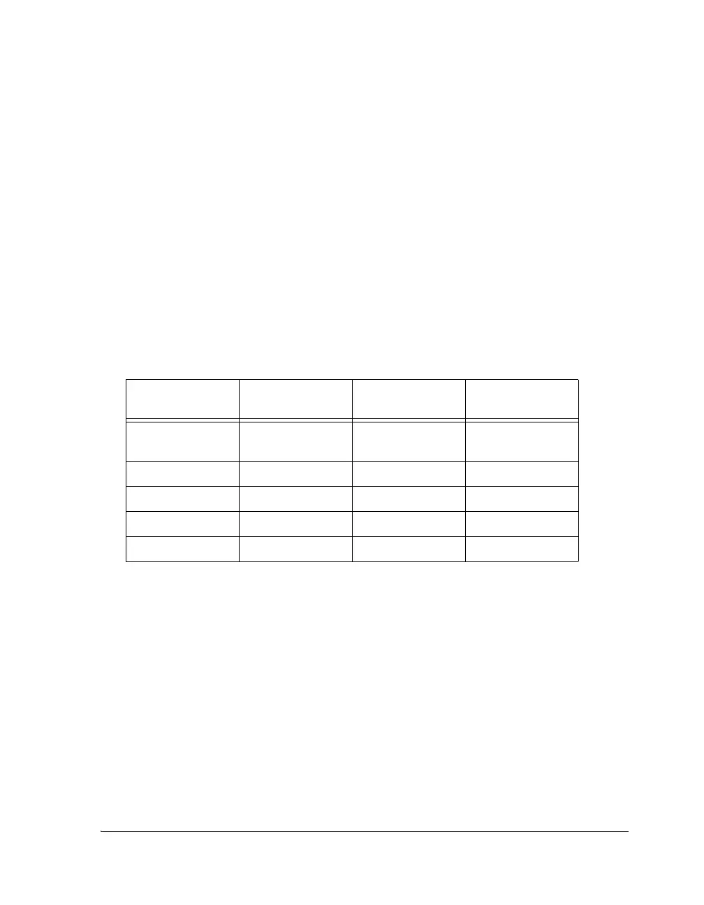
Table 3-13. SDC Clock Frequencies
CK/SDCLK Clock
Period Ratio
SDRAM Frequency
(400 MHZ)
SDRAM Frequency
(333 MHZ)
SDRAM Frequency
(266 MHZ)
1:2.0 166
(not supported)
166 133
1:2.5 160 133 106
1:3.0 133 111 88
1:3.5 114 95 76
1:4.0 100 83 66
 Loading...


