SPORT Control Registers and Data Buffers
5-58 ADSP-21368 SHARC Processor Hardware Reference
In the ADSP-21367/8/9 and ADSP-2137x processors, there is one global
interrupt status register,
SPERRSTAT, that checks the status of SPORT
interrupts. This read-only register is located at address 0x2300 and is 24
bits wide.
Register Writes and Effect Latency
SPORT register writes are internally completed at the end of five (worst
case) or four (best case) core clock cycles. The newly written value to the
SPORT register can be read back on the next cycle. Reads of the SPORT
registers take four core clock cycles.
After a write to a SPORT register, control and mode bit changes take
effect in the second serial clock cycle. The SPORTs are ready to start
transmitting or receiving three serial clock cycles after they are enabled in
the
SPCTLx control registers. No serial clocks are lost from this point on.
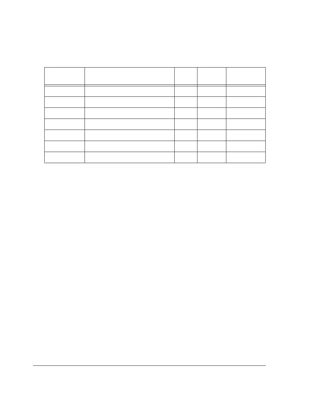
RX6A Receiver FIFO Register in SP6A 32 1 04861
TX6B Transmitter FIFO Register in SP6B 32 1 04862
RX6B Receiver FIFO Register in SP6B 32 1 04863
TX7A Transmitter FIFO Register in SP7A 32 1 04864
RX7A Receiver FIFO Register in SP37A 32 1 04867
TX7B Transmitter FIFO Register in SP7B 32 1 04866
RX7B Receiver FIFO Register in SP7B 32 1 04867
Table 5-8. SPORT6 and SPORT7 Registers (Cont’d)
Register Name Function Width No. of
Registers
Memory Map
[17:0]
 Loading...


