ADSP-21368 SHARC Processor Hardware Reference 3-11
External Port
throughput is maximized when SDRAM is programmed to run at half the
core clock frequency and the instructions being fetched are sequential.
After the initial latency, accesses follow a 4-2-4-2-4 core cycles pattern for
the above setting for a 32-bit SDRAM meaning that because of the way
the instructions are packed in external memory, the first instruction takes
four core clock cycles to execute, while the second instruction only takes
two core cycles, and so on.
It is possible to store both 48-bit instructions as well as 32-bit data in the
external memory bank 0. However, care must be taken while specifying
the proper starting addresses if 48-bit instructions are stored or interleaved
with 32-bit data in the same memory bank. For example, in case of 32-bit
wide external SDRAM memory, two instructions are packed into three
32-bit memory locations, while 32-bit data occupies one memory location
each. If 2K instructions are placed starting at the bank 0 base address
(0x0020 0000), then the starting address for placing data has to be at least
0x0020 0C00 (in other words, an offset of 3K 32-bit words).
The ADSP-2137x processors support the execution of 48-bit wide pro-
gram instructions from external memory devices of various widths. The
processor can transparently pack and execute instructions stored in 16-bit
(ADSP-21375) or 32-bit wide (ADSP-21371) external memory.
Table 3-3 shows the format of stored instructions in external 32-bit wide
memory. The sequencer automatically places the normal word address
corresponding to the starting address of the first instruction to be fetched
from external memory on the appropriate address bus, fetches three 16-bit
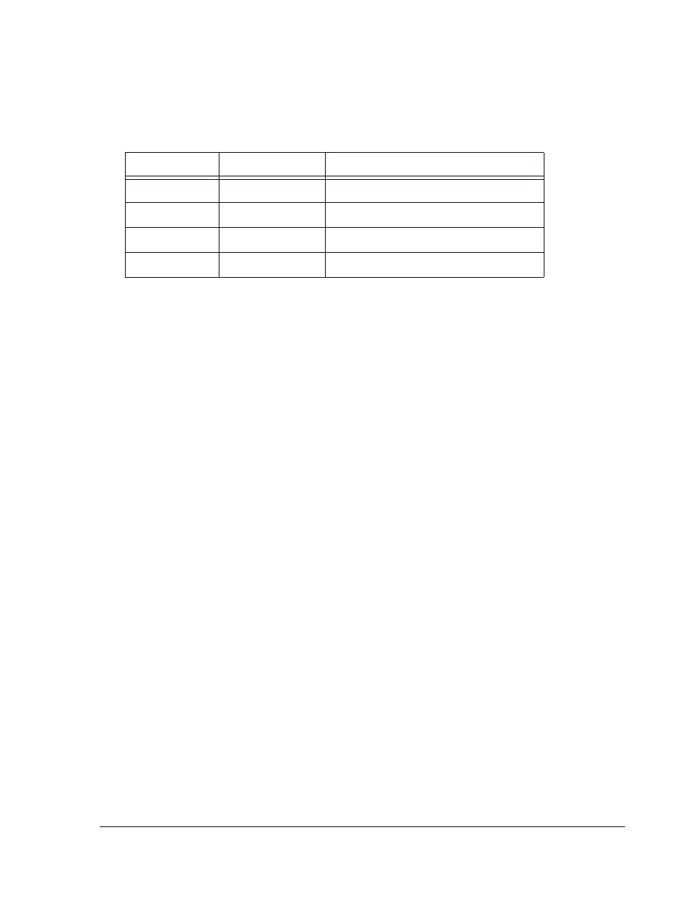
Table 3-2. External Address Space for SDRAM Memory Accesses
Bank Size in words Address Range
Bank 0 62M 0x0020 0000 – 0x03FF FFFF
Bank 1 64M 0x0400 0000 – 0x07FF FFFF
Bank 2 64M 0x0800 0000 – 0x0BFF FFFF
Bank 3 64M 0x0C00 0000 – 0x0FFF FFFF
 Loading...


