External Memory Interface
3-10 ADSP-21368 SHARC Processor Hardware Reference
The address range of external memory (asynchronous memory) is shown
in Table 3-1. External bank 0 can be used to execute instructions.
Table 3-2 shows the addressable range for SDRAM memory space. Bank 0
can be used for executing instructions. Note that the external memory
bank addresses shown are for normal word accesses.
The actual throughput execution from external SDRAM is dependent on
the configuration of the SDRAM. The SDRAM can be programmed to
run at a number of different frequency ratios with respect to the core
clock, the fastest being half of the core clock (or the same as the peripheral
clock). The core and SDRAM controller have been enhanced so that
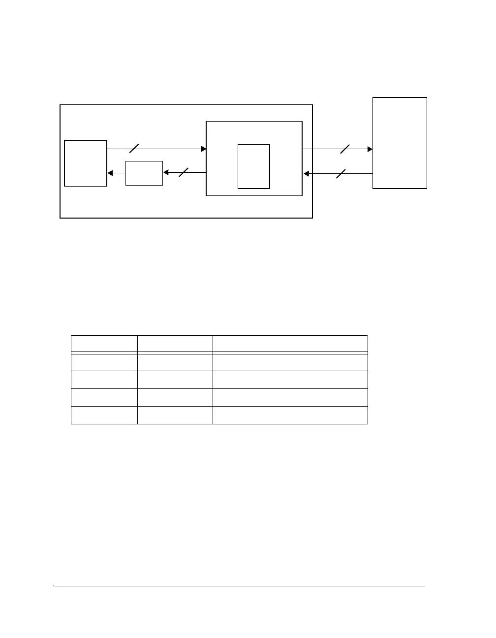
Figure 3-3. Logical Versus Physical Addresses
Table 3-1. External Memory Address Space for Non SDRAM Addresses
Bank Size in words Address Range
Bank 0 14M 0x0020 0000 – 0x00FF FFFF
Bank 1 16M 0x0400 0000 – 0x04FF FFFF
Bank 2 16M 0x0800 0000 – 0x08FF FFFF
Bank 3 16M 0x0C00 0000 – 0x0CFF FFFF
External
ADSP-213xx
Port
External
Bank 0
Sequencer
Packing
Unit
48
24
“Physical
Address” on
address bus
16/32 bit*
“Instruction Data”
on data bus
*32-bit on the ADSP-21371 and
16-bit on the ADSP-21375.
“Logical
Address”
24
Data
Address
Memory
Address
Translator
 Loading...


