S/PDIF Transmitter
9-8 ADSP-21368 SHARC Processor Hardware Reference
The S/PDIF transmitter output may be routed to an output pin through
SRU1 and then routed to another S/PDIF receiver or to components for
off-board connections to other S/PDIF receivers. The output is also avail-
able to the S/PDIF receiver for loop-back testing through SRU1.
Two output data formats are supported by the transmitter: two channel
mode and single channel double frequency (SCDF) mode. The output for-
mat is determined by the transmitter control register (
DITCTL). For more
information, see “Transmitter Control Register (DITCTL)” on
page A-86.
In two channel mode, the left channel (channel A) is transmitted when the
LRCLK is high and the right channel (channel B) is transmitted when the
LRCLK is low.
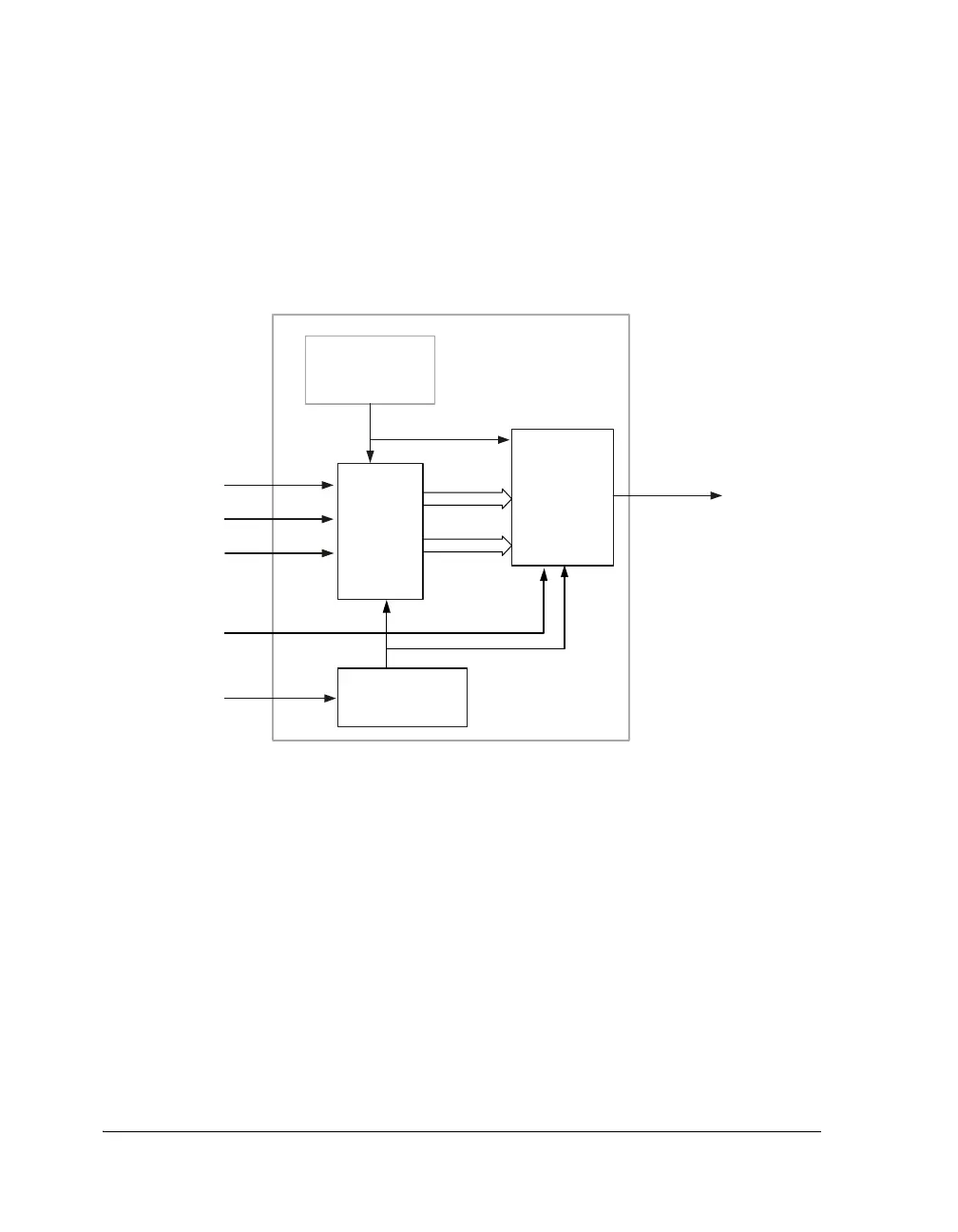
Figure 9-4. S/PDIF Transmitter Block Diagram
TRANSMITTER
CONTROL
REGISTER
SERIAL TO
PARALLEL
CONVERTER
TRANSMITTER
BI-PHASE
CLOCK
GENERATOR
SCLK (BCLK)
SDATA
LRCLK (FS)
TX_CLK
TX_BI-PHASE_CLOCK
BI-PHASE_OUT
AUDIO
SAMPLES
CONTROL
EXT_SYNC
 Loading...


