Programming Examples
13-18 ADSP-21368 SHARC Processor Hardware Reference
In the following example code, the most significant two bits of the control
registers (
PCG_CTLx) specify the clock source and enable the clock genera-
tors. Set the clock divisor and source and low phase word first, followed by
the control register enable bits, which must be set together. When the
PCG_PW register is set to 0 (default) the FS pulse width is divisor/2 for even
divisors and (divisor – 1)/2 for odd divisors. Alternatively, the PCG_PW reg-
ister could be set high for exactly half the period of
CLKIN cycles for a 50%
duty cycle, provided the
FSYNC divisor is an even number.
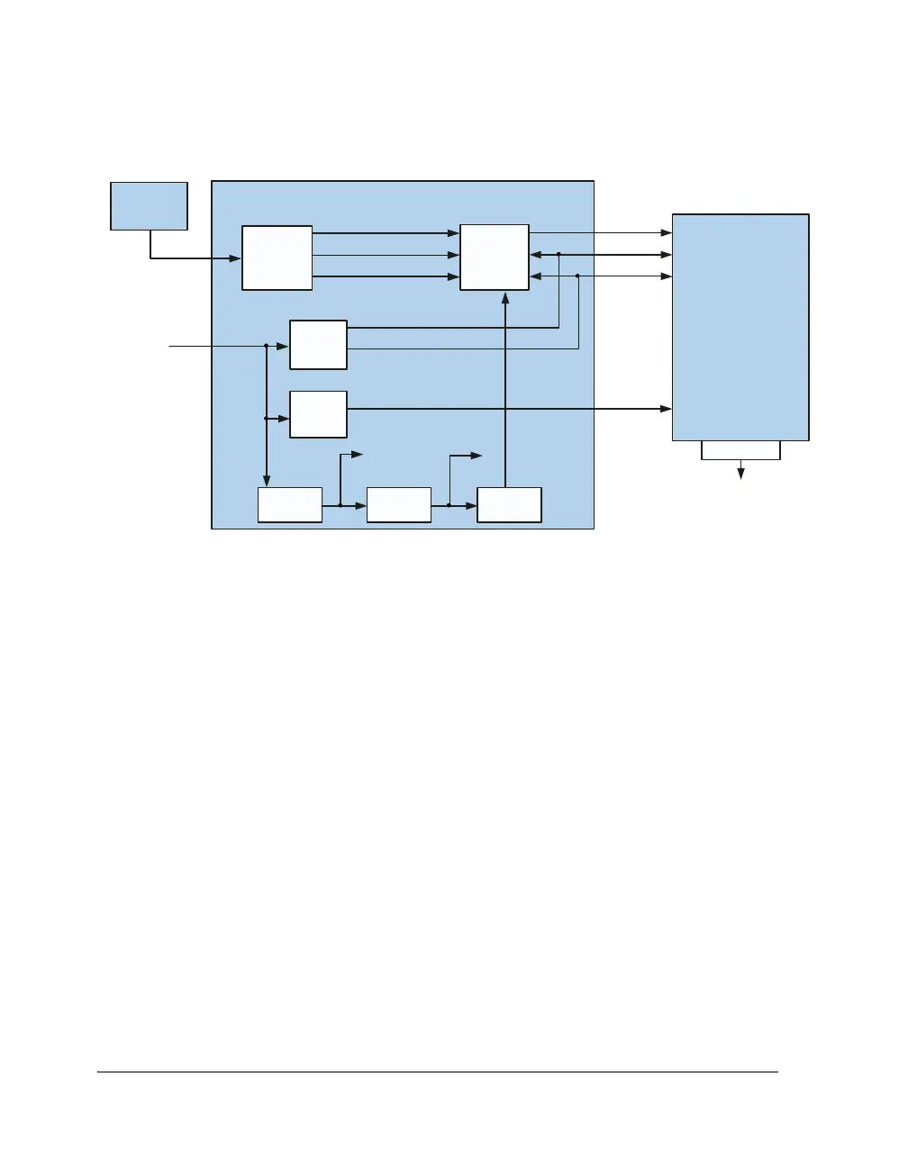
Figure 13-6. PCG Setup for I
2
S or Left-Justified DAI
ADSP-21369
S/PDIF
Rx
SRC
RxSCLK
RxLRCLK
SDATA
IN
PCG
A
PCG
B
PLL CCLK ÷ 2 CCLK ÷ 4
CCLK
(242 MHz)
HCLK
(121 MHz)
SDATA
OUT
DAI_P8
DAI_P9
DAI_P10
STEREO DAC
LEFT
OUT
RIGHT
OUT
MCLK
IN
DAI_P11
MCLK
(30 MHz)
FSYNC
A
(FS
OUT
) ÷ 512 = 65.1 kHz
SCLK
A
(64 FS
OUT
)÷8=4.167MHz
MCLK
B
(256 FS
OUT
) ÷ 2 = 16.67 MHz
F
CLKIN
(33.330 MHz)
S/PDIF
IN
(FS
IN
,44.1kHz
DAI_P19
SDATA
IN
LRCLK
IN
SCLK
IN
FS
OUT
= 65.1 kHz
24-BIT, LEFT-JUSTIFIED
CD
PLAYER
HEAD PHONES
 Loading...


