Precision Clock Generator Registers
A-162 ADSP-21368 SHARC Processor Hardware Reference
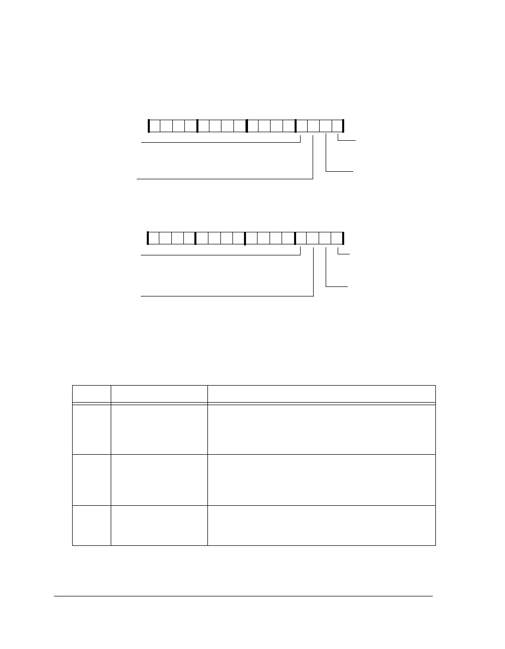
Figure A-78. PCG_SYNC2 Register
Table A-68. PCG_SYNC2 Register Bit Descriptions
Bit Name Description
0FSC_SYNC Enable synchronization of frame sync C with external
frame sync.
0 = Frame sync disabled
1 = Frame sync enabled
1CLKC_SYNC Enable synchronization of clock C with external frame
sync.
0 = Clock disabled
1 = Clock enabled
2CLKC_SOURCE_IOPEnable clock C input source.
0 = XTAL buffer output selected for clock C
1 = EXT_CLKA_I selected for clock C
31 30 29 28 27 26 25 24 23 22 21 20 19 18 17 16
0000000000000000
15 14 13 12 11 10 9 8 7 6 5 4 3 2 1 0
0000000000000000
PCG_SYNC2 (0x24CB)
Enable synchronization of
FSD with external LRCLK
FSD_SYNC
FSC_SOURCE_IOP
Enable frame sync C input source.
0 = XTAL buffer output selected for frame sync C
1 = EXT_CLKA_I selected for frame sync C
Enable synchronization of
FSC with external LRCLK
FSC_SYNC
Enable synchronization of clock
C with external LRCLK
CLKC_SYNC
CLKC_SOURCE_IOP
Enable clock C input source.
0 = XTAL buffer output selected for clock C
1 = EXT_CLKA_I selected for clock C
Enable synchronization of
clock D with external LRCLK
CLKD_SYNC
FSD_SOURCE_IOP
CLKD_SOURCE_IOP
Enable clock D input source.
0 = XTAL buffer output selected for clock D
1 = EXT_CLKA_I selected for clock D
Enable frame sync D input source.
0 = XTAL buffer output selected for frame sync D
1 = EXT_CLKA_I selected for frame sync D
 Loading...


