ADSP-21368 SHARC Processor Hardware Reference 14-7
System Design
Case 5
If no external memory is used, and if the PDAP data lines are connected
to DATA pins, and if 8 flags are required, then use MODE 6. Connect
the PADP control lines to the DATA pins, and program the flag direction
in the
FLAGS register.
The upper 32 data pins of the external memory interface are muxed (using
bits 23–21 in the SYSCTL register) to support the external memory inter-
face data (input/output), the PDAP (input only), the FLAGS
(input/output), and the PWM channels (output). Table 14-1 provides the
pin settings for these functions.
In PDAP mode, the DATA pins function as follows.
•
DATA12–31 pins act as PDAP0–19 (inputs)
• DATA11 pin acts as PDAP HLD (input)
•
DATA10 pin acts as PDAP CLK (input)
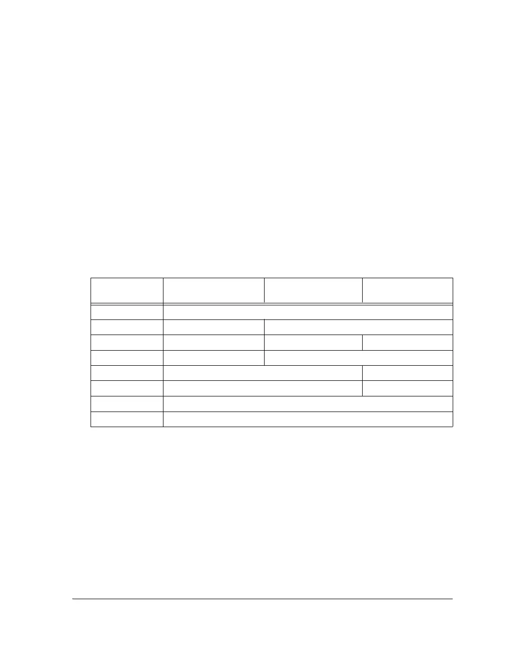
Table 14-1. Function of Data Pins
SYSCTL bits
23–21 Settings
DATA31–16
1
1 Not available on the ADSP-21375 processor.
DATA15–8 DATA7–0
000 EPDATA32–0 (default at RESET)
001 FLAGS/PWM15–0
2
2 These signals can be FLAGS or PWM or a mix of both. However, they can be selected only in
groups of four. Their function is determined by the control signals FLAGS/PWM_SEL.
EPDATA15–0
010 FLAGS/PWM15–0
1
FLAGS15–8 EPDATA7–0
011 FLAGS/PWM15–0
1
FLAGS15–0
100 PDAP (DATA + CTRL) EPDATA7–0
101 PDAP (DATA + CTRL) FLAGS7–0
110 Reserved
111 Three-state all pins
 Loading...


