ADSP-21368 SHARC Processor Hardware Reference A-11
Register Reference
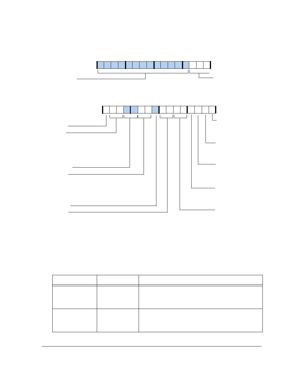
Figure A-4. External Port Control Register
Table A-3. EPCTL Register Bit Descriptions
Bit Name Description
0B0SDSelect Bank 0 SDRAM.
1 = Bank 0 SDRAM
0 = Bank 0 Non-SDRAM
1B1SDSelect Bank 1 SDRAM.
1 = Bank 1 SDRAM
0 = Bank 1 Non-SDRAM
15 14 13 12 11 10 8 7 6 5 4 3 2 1 0
0000000000000000
DATE
9
EPCTL (0x1801)
31 30 29 28 27 26 25 24 23 22 21 20 19 18 17 16
0000000000000000
B0SD
Bank 0 SDRAM
1=Bank 0 SDRAM
0=Bank 0 Non-SDRAM
Reserved
B1SD
Bank 1 SDRAM
1=Bank 1 SDRAM
0=Bank 1 Non-SDRAM
B2SD
Bank 2 SDRAM
1=Bank 2 SDRAM
0=Bank 2 Non-SDRAM
B0SD
Bank 3 SDRAM
1=Bank 3 SDRAM
0=Bank 3 Non-SDRAM
DMAPR
DMA Channel Priority for CH0 and CH1
11 = Rotating priority
10 = Fixed priority
01 = Reserved
00 = Reserved
EPBR
External Port Bus Priority
11=Rotating Priority
10=Core has high priority
01=DMA has high priority
00=Reserved
FRZDMA
Arbitration Freezing Length for DMA
0=No freezing
1=4 Accesses
2=8 Accesses
3=16 Accesses
FRZCR
Arbitration Freezing Length for CORE
Accesses
0 = No Freezing
1 = 4 Accesses
2 = 8 Accesses
3 = 16 Accesses
DATE
DATA Enable
In no pack mode, masks
those bits of the data lane
with zeros.
Reserved
Reserved
 Loading...


