R01UH0823EJ0100 Rev.1.00 Page 1429 of 1823
Jul 31, 2019
RX23W Group 40. SD Host Interface (SDHIa)
40.2.7 SD Status Register 2 (SDSTS2)
Note 1. The flag does not change even if set to 1. Writing 0 changes the flag value to 0.
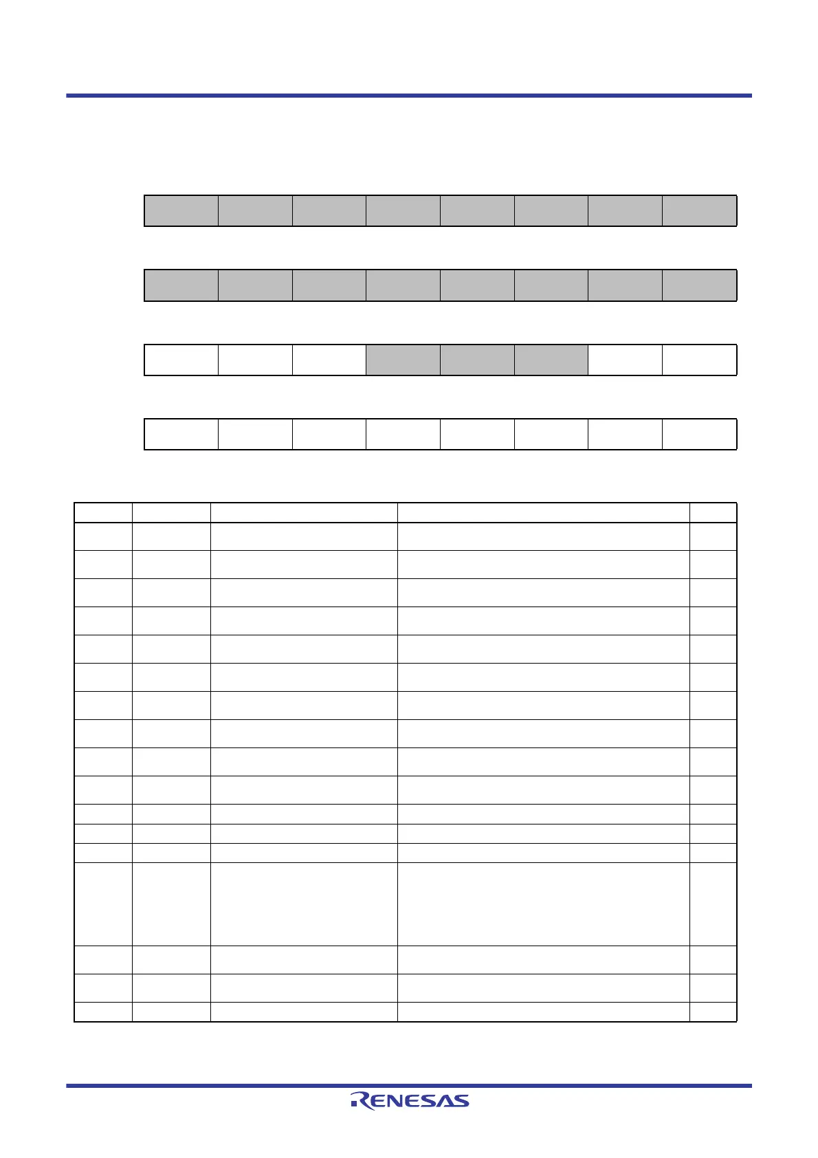
SDSTS2
Address(es): SDHI.SDSTS2 0008 AC3Ch
b31 b30 b29 b28 b27 b26 b25 b24
— — — — — — — —
Value after reset:
00000000
b23 b22 b21 b20 b19 b18 b17 b16
— — — — — — — —
Value after reset:
00000000
b15 b14 b13 b12 b11 b10 b9 b8
ILA CBSY SDCLKCREN — — —BWEBRE
Value after reset:
00100000
b7 b6 b5 b4 b3 b2 b1 b0
SDD0MON RSPTO ILR ILW DTO ENDE CRCE CMDE
Value after reset:
x0000000
Bit Symbol Bit Name Description R/W
b0 CMDE Command Error Detection Flag
0: Command error not detected
1: Command error detected
R/(W)
*1
b1 CRCE CRC Error Detection Flag
0: CRC error not detected
1: CRC error detected
R/(W)
*1
b2 ENDE End Bit Error Detection Flag
0: End bit error not detected
1: End bit error detected
R/(W)
*1
b3 DTO Data Timeout Detection Flag
0: Data timeout not detected
1: Data timeout detected
R/(W)
*1
b4 ILW
SDBUFR Illegal Write Access
Detection Flag
0: Illegal write access to the SDBUFR register not detected
1: Illegal write access to the SDBUFR register detected
R/(W)
*1
b5 ILR
SDBUFR Illegal Read Access
Detection Flag
0: Illegal read access to the SDBUFR register not detected
1: Illegal read access to the SDBUFR register detected
R/(W)
*1
b6 RSPTO Response Timeout Detection Flag
0: Response timeout not detected
1: Response timeout detected
R/(W)
*1
b7 SDD0MON SDHI_D0 Pin Status Flag
0: SDHI_D0 pin is low
1: SDHI_D0 pin is high
R
b8 BRE SDBUFR Read Enable Flag
0: Read access to the SDBUFR register disabled
1: Read access to the SDBUFR register enabled
R/(W)
*1
b9 BWE SDBUFR Write Enable Flag
0: Write access to the SDBUFR register disabled
1: Write access to the SDBUFR register enabled
R/(W)
*1
b10 — Reserved This bit is 0 when read and cannot be modified. R
b11 — Reserved This bit is 0 when read. Set it to 1 when writing. R/W
b12 — Reserved This bit is 0 when read and cannot be modified. R
b13 SDCLKCREN SDCLKCR Write Enable Flag
0: SD bus (CMD and DAT lines) is busy, so write access to
the SDCLKCR.CLKEN bit and CLKSEL[7:0] bits is
disabled.
1: SD bus (CMD and DAT lines) is not busy, so write
access to the SDCLKCR.CLKEN bit and CLKSEL[7:0]
bits is enabled.
R
b14 CBSY Command Sequence Status Flag
0: Command sequence completed
1: Command sequence in progress (busy)
R
b15 ILA Illegal Access Error Detection Flag
0: Illegal access error not detected
1: Illegal access error detected
R/(W)
*1
b31 to b16 — Reserved These bits are 0 when read and cannot be modified. R

 Loading...


