R01UH0823EJ0100 Rev.1.00 Page 503 of 1823
Jul 31, 2019
RX23W Group 23. Multi-Function Timer Pulse Unit 2 (MTU2a)
23.2.16 Timer Output Master Enable Registers (TOER)
Note 1. To output a non-active level from each pin when MTU output is disabled, make necessary settings for non-active level output
from general I/O ports in the data direction registers (PDR), port output data registers (PODR), and port mode register (PMR) in
advance. For details, refer to the I/O Ports section.
The TOER registers enable or disable output settings for output pins MTIOC4D, MTIOC4C, MTIOC3D, MTIOC4B,
MTIOC4A, and MTIOC3B.
These pins do not output correctly if the bits in the TOER register have not been set. In MTU3 and MTU4, set the TOER
register prior to setting the TIOR register.
Set the TOER register after setting the TSTR.CST3 and CST4 bits to 0 (refer to
Figure 23.35 and Figure 23.38).
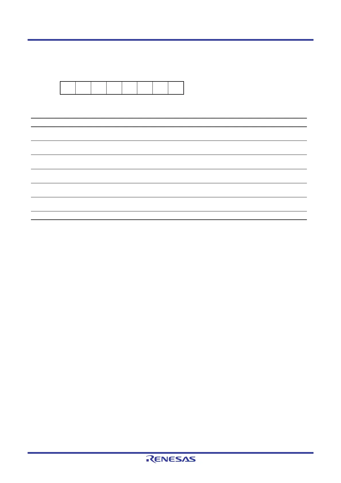
Address(es): MTU.TOER 000D 0A0Ah
b7 b6 b5 b4 b3 b2 b1 b0
— — OE4D OE4C OE3D OE4B OE4A OE3B
Value after reset:
11000000
Bit Symbol Bit Name Description R/W
b0 OE3B Master Enable MTIOC3B 0: MTU output is disabled*
1
1: MTU output is enabled
R/W
b1 OE4A Master Enable MTIOC4A 0: MTU output is disabled*
1
1: MTU output is enabled
R/W
b2 OE4B Master Enable MTIOC4B 0: MTU output is disabled*
1
1: MTU output is enabled
R/W
b3 OE3D Master Enable MTIOC3D 0: MTU output is disabled*
1
1: MTU output is enabled
R/W
b4 OE4C Master Enable MTIOC4C 0: MTU output is disabled*
1
1: MTU output is enabled
R/W
b5 OE4D Master Enable MTIOC4D 0: MTU output is disabled*
1
1: MTU output is enabled
R/W
b7, b6 — Reserved These bits are read as 1. The write value should be 1. R/W

 Loading...


