R01UH0823EJ0100 Rev.1.00 Page 986 of 1823
Jul 31, 2019
RX23W Group 33. Serial Communications Interface (SCIg, SCIh)
33.2.10 Smart Card Mode Register (SCMR)
Note 1. Writable only when TE in SCR = 0 and RE in SCR = 0 (both serial transmission and reception are disabled).
Note 2. The setting is invalid and a fixed data length of 8 bits is used in modes other than asynchronous mode.
Note 3. LSB first should be selected and the value of MSB (b7) in the TDR register cannot be transmitted.
SMIF Bit (Smart Card Interface Mode Select)
When this bit is set to 1, smart card interface mode is selected.
When this bit is set to 0, non-smart card interface mode, i.e., asynchronous mode (including multi-processor mode),
clock synchronous mode, simple SPI mode, or simple I
2
C mode is selected.
SINV Bit (Transmitted/Received Data Invert)
Inverts the transmit/receive data logic level. This bit does not affect the logic level of the parity bit. To invert the parity
bit, invert the PM bit in the SMR register.
CHR1 Bit (Character Length 1)
Selects the data length of transmit/receive data.
Selects in combination with the CHR bit in SMR.
A fixed data length of 8 bits is used in modes other than asynchronous mode.
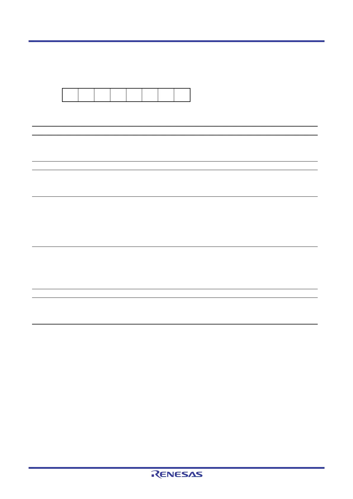
Address(es): SCI1.SCMR 0008 A026h, SCI5.SCMR 0008 A0A6h, SCI8.SCMR 0008 A106h, SCI12.SCMR 0008 B306h,
SMCI1.SCMR 0008 A026h, SMCI5.SCMR 0008 A0A6h, SMCI8.SCMR 0008 A106h, SMCI12.SCMR 0008 B306h
b7 b6 b5 b4 b3 b2 b1 b0
BCP2 — — CHR1 SDIR SINV — SMIF
Value after reset:
11110010
Bit Symbol Bit Name Description R/W
b0 SMIF Smart Card Interface Mode
Select
0: Non-smart card interface mode
(Asynchronous mode, clock synchronous mode, simple SPI mode,
or simple I
2
C mode)
1: Smart card interface mode
R/W*
1
b1 — Reserved This bit is read as 1. The write value should be 1. R/W
b2 SINV Transmitted/Received Data
Invert
0: TDR contents are transmitted as they are. Receive data is stored as
it is in RDR.
1: TDR contents are inverted before being transmitted. Receive data is
stored in inverted form in RDR.
R/W*
1
b3 SDIR Transmitted/Received Data
Transfer Direction
This bit can be used in the following modes.
Smart card interface mode
Asynchronous mode (multi-processor mode)
Clock synchronous mode
Simple SPI mode
Set this bit to 1 if operation is to be in simple I
2
C mode.
0: Transfer with LSB first
1: Transfer with MSB first
R/W*
1
b4 CHR1 Character Length 1 (Only valid in asynchronous mode)*
2
Selects in combination with the SMR.CHR bit.
CHR1 CHR
0 0: Transmit/receive in 9-bit data length
0 1: Transmit/receive in 9-bit data length
1 0: Transmit/receive in 8-bit data length (initial value)
1 1: Transmit/receive in 7-bit data length*
3
R/W*
1
b6, b5 — Reserved These bits are read as 1. The write value should be 1. R/W
b7 BCP2 Base Clock Pulse 2 Selects the number of base clock cycles in combination with the
SMR.BCP[1:0] bits.
Table 33.9 lists the combinations of the SCMR.BCP2 bit and
SMR.BCP[1:0] bits.
R/W*
1

 Loading...


