R01UH0823EJ0100 Rev.1.00 Page 855 of 1823
Jul 31, 2019
RX23W Group 32. USB 2.0 Host/Function Module (USBc)
32.2 Register Descriptions
32.2.1 System Configuration Control Register (SYSCFG)
Note 1. Do not enable the DMRPU and DPRPU bits at the same time.
Note 2. After writing 1 to the SCKE bit, read it and confirm it is set to 1.
USBE Bit (USB Operation Enable)
The USBE bit enables or disables operation of the USB.
Modifying the USBE bit from 1 to 0 initializes the register bits listed in
Table 32.3.
This bit should be modified while the SCKE bit is 1.
When the host controller is selected, this bit should be set to 1 after setting the DRPD bit to 1, eliminating
SYSSTS0.LNST[1:0] flag chattering, and confirming that the USB bus state is stabilized.
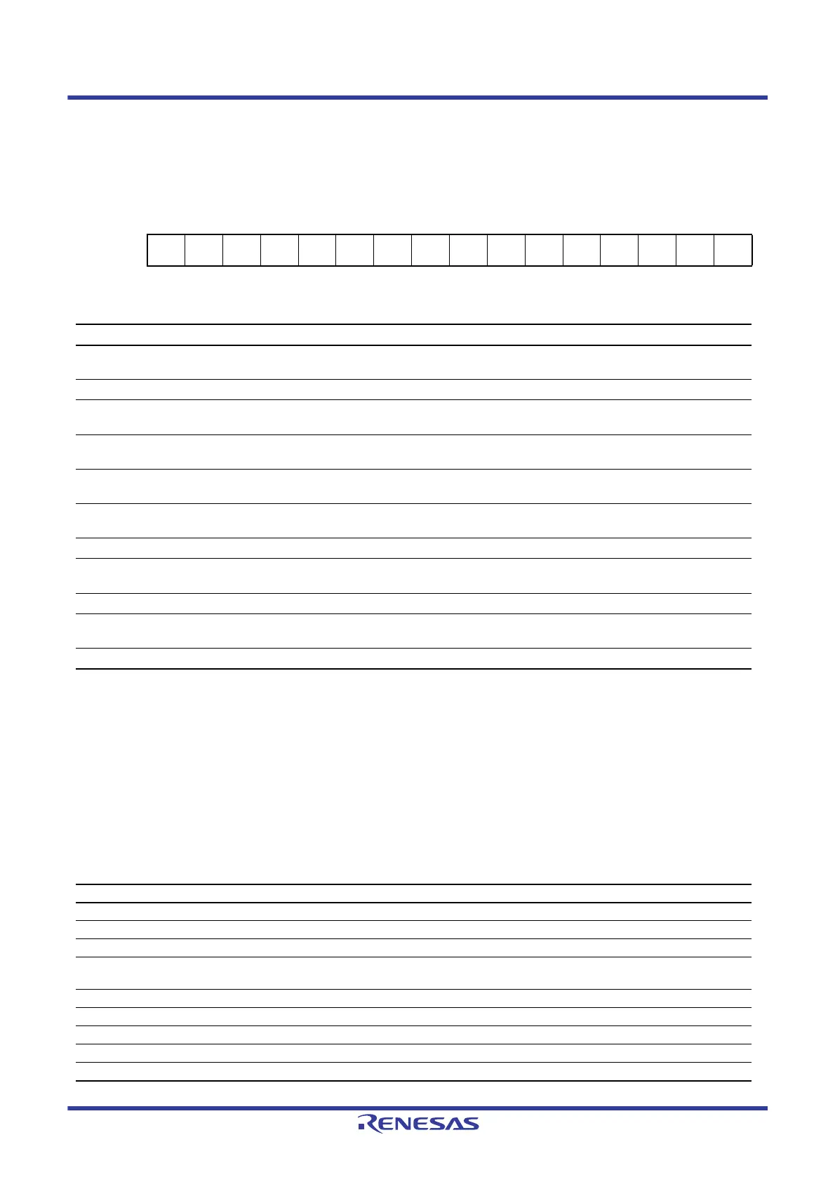
Address(es): 000A 0000h
b15 b14 b13 b12 b11 b10 b9 b8 b7 b6 b5 b4 b3 b2 b1 b0
—————SCKE—CNEN—DCFMDRPDDPRPU
DMRP
U
— — USBE
Value after reset:
0000000000000000
Bit Symbol Bit Name Description R/W
b0 USBE USB Operation Enable 0: USB operation is disabled.
1: USB operation is enabled.
R/W
b2, b1 — Reserved These bits are read as 0. The write value should be 0. R/W
b3 DMRPU D– Line Resistor Control*
1
0: Pulling up the line is disabled.
1: Pulling up the line is enabled.
R/W
b4 DPRPU D+ Line Resistor Control*
1
0: Pulling up the line is disabled.
1: Pulling up the line is enabled.
R/W
b5 DRPD D+/D– Line Resistor Control 0: Pulling down the lines is disabled.
1: Pulling down the lines is enabled.
R/W
b6 DCFM Controller Function Select 0: Function controller is selected.
1: Host controller is selected.
R/W
b7 — Reserved This bit is read as 0. The write value should be 0. R/W
b8 CNEN CNEN Single End Receiver
Enable
0: Single end receiver operation is disabled.
1: Single end receiver operation is enabled.
R/W
b9 — Reserved This bit is read as 0. The write value should be 0. R/W
b10 SCKE USB Clock Enable*
2
0: Stops supplying the clock signal to the USB.
1: Enables supplying the clock signal to the USB.
R/W
b15 to b11 — Reserved These bits are read as 0. The write value should be 0. R/W
Table 32.3 Registers Initialized by Writing 0 to the SYSCFG.USBE Bit
Selected Function Register Bit Remarks
Function controller SYSSTS0 LNST[1:0] The value is retained when the host controller is selected.
DVSTCTR0 RHST[2:0]
INTSTS0 DVSQ[2:0] The value is retained when the host controller is selected.
USBREQ BREQUEST[7:0],
BMREQUESTTYPE[7:0]
The value is retained when the host controller is selected.
USBVAL — The value is retained when the host controller is selected.
USBINDX — The value is retained when the host controller is selected.
USBLENG — The value is retained when the host controller is selected.
Host controller DVSTCTR0 RHST[2:0]
FRMNUM FRNM[10:0] The value is retained when the function controller is selected.

 Loading...


