R01UH0823EJ0100 Rev.1.00 Page 649 of 1823
Jul 31, 2019
RX23W Group 24. Port Output Enable 2 (POE2a)
24.2.6 Port Output Enable Control Register 2 (POECR2)
Note 1. Can be modified only once after a reset.
When this function is not used, write 00h to this register.
P3CZEA Bit (MTU Port 3 High-Impedance Enable)
This bit gives permission regarding whether or not the MTIOC4B and MTIOC4D pins for complementary PWM output
from the MTU are placed in the high-impedance. It also gives permission regarding whether or not the levels on the
MTIOC4B and MTIOC4D pins are compared.
P2CZEA Bit (MTU Port 2 High-Impedance Enable)
This bit gives permission regarding whether or not the MTIOC4A and MTIOC4C pins for complementary PWM output
from the MTU are placed in the high-impedance. It also gives permission regarding whether or not the levels on the
MTIOC4A and MTIOC4C pins are compared.
P1CZEA Bit (MTU Port 1 High-Impedance Enable)
This bit gives permission regarding whether or not the MTIOC3B and MTIOC3D pins for complementary PWM output
from the MTU are placed in the high-impedance. It also gives permission regarding whether or not the levels on the
MTIOC3B and MTIOC3D pins are compared.
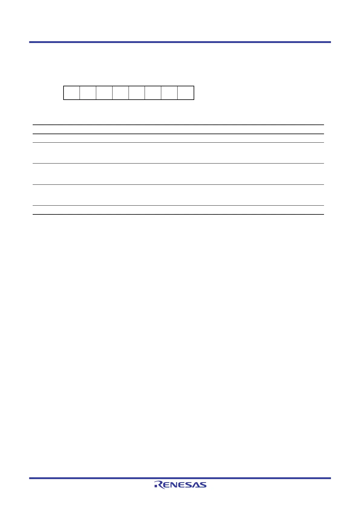
Address(es): 0008 890Ch
b7 b6 b5 b4 b3 b2 b1 b0
—
P1CZE
A
P2CZE
A
P3CZE
A
————
Value after reset:
01110000
Bit Symbol Bit Name Description R/W
b3 to b0 — Reserved These bits are read as 0. The write value should be 0. R/W
b4 P3CZEA MTU Port 3 High-Impedance
Enable
0: Comparison of output levels does not proceed and the
pins are not placed in the high-impedance.
1: The pins are placed in the high-impedance.
R/W*
1
b5 P2CZEA MTU Port 2 High-Impedance
Enable
0: Comparison of output levels does not proceed and the
pins are not placed in the high-impedance.
1: The pins are placed in the high-impedance.
R/W*
1
b6 P1CZEA MTU Port 1 High-Impedance
Enable
0: Comparison of output levels does not proceed and the
pins are not placed in the high-impedance.
1: The pins are placed in the high-impedance.
R/W*
1
b7 — Reserved This bit is read as 0. The write value should be 0. R/W

 Loading...


