R01UH0823EJ0100 Rev.1.00 Page 1367 of 1823
Jul 31, 2019
RX23W Group 38. Serial Peripheral Interface (RSPIa)
38.3.4.1 When Parity is Disabled (SPCR2.SPPE = 0)
When parity is disabled, data for transmission are copied to the shift register with no prior processing. A description of
the connection between the RSPI data register (SPDR) and the shift register in terms of the combination of MSB or LSB
first and data length is given below.
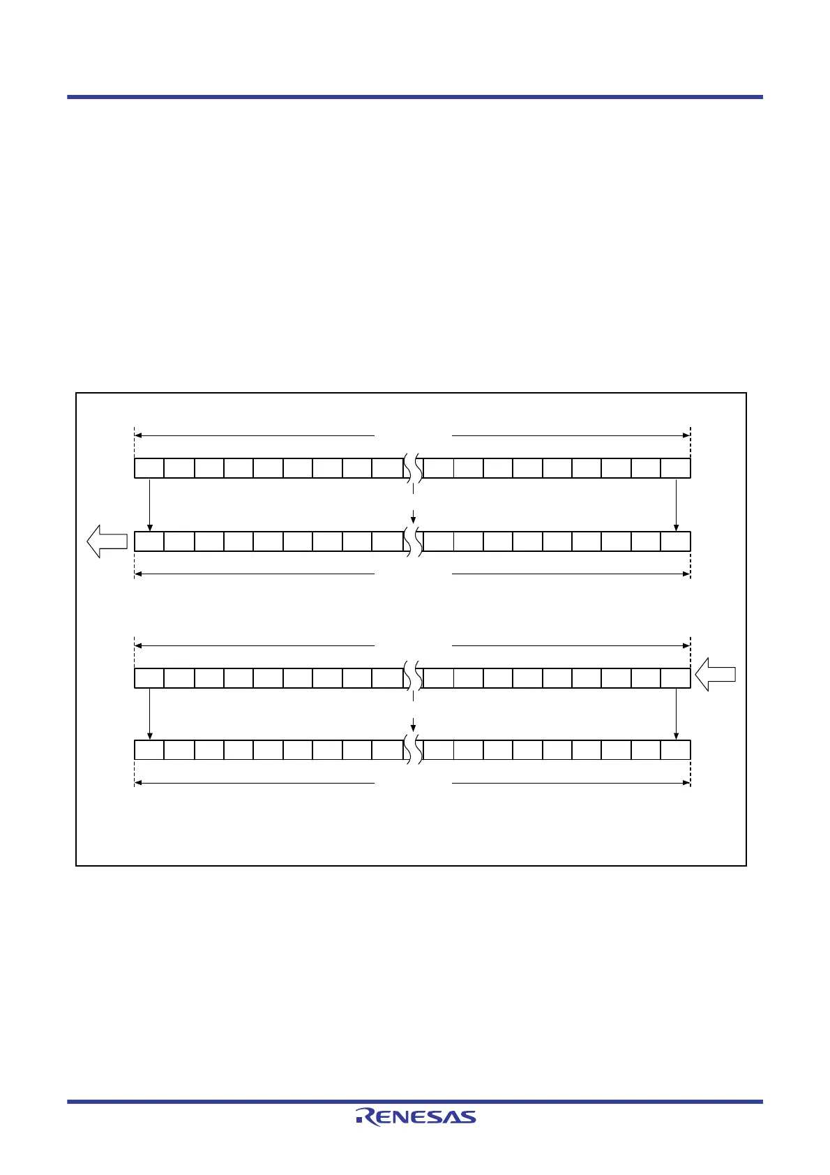
(1) MSB First Transfer (32-Bit Data)
Figure 38.14 shows details of operations by the RSPI data register (SPDR) and the shift register in transfer with parity
disabled, an RSPI data length of 32 bits, and MSB first selected.
In transmission, bits T31 to T00 from the current stage of the transmit buffer are copied to the shift register. Data for
transmission are shifted out from the shift register in order from T31, through T30, and so on to T00.
In reception, received data are shifted in bit by bit through bit 0 of the shift register. When bits R31 to R00 have been
collected after input of the required number of cycles of RSPCK, the value in the shift register is copied to the receive
buffer.
Figure 38.14 MSB First Transfer (32-Bit Data, Parity Disabled)
Bit 31
Transfer start
Transfer end
Bit 0
T31 T30 T29 T28 T27 T26 T25 T24 T23 T06 T05 T04 T03 T02 T01 T00
T31 T30 T29 T28 T27 T26 T25 T24 T23 T06 T05 T04 T03 T02 T01 T00
R31 R30 R29 R28 R27 R26 R25 R24 R23 R06 R05 R04 R03 R02 R01 R00
R31 R30 R29 R28 R27 R26 R25 R24 R23 R06 R05
T08 T07
T08 T07
R08 R07
R08 R07 R04 R03 R02 R01 R00
Transmit buffer
Shift register
Copy
Shift register
Input
Output
Copy
Bit 0
Bit 0
Bit 0
Receive buffer
Bit 31
Bit 31
Bit 31
Note: Output = MOSI (master)/MISO (slave), input = MISO (master)/MOSI (slave)

 Loading...


