R01UH0823EJ0100 Rev.1.00 Page 175 of 1823
Jul 31, 2019
RX23W Group 9. Clock Generation Circuit
9.2.3 PLL Control Register (PLLCR)
Note: Set the PRCR.PRC0 bit to 1 (write enabled) before rewriting this register.
Writing to the PLLCR is prohibited when the PLLCR2.PLLEN bit is 0 (PLL is operating).
PLIDIV[1:0] Bits (PLL Input Frequency Division Ratio Select)
These bits select the frequency division ratio of the PLL clock source.
Set these bits so that the frequency of PLL input signal is within the range of 4 MHz to 12.5 MHz.
STC[5:0] Bits (Frequency Multiplication Factor Select)
These bits select the frequency multiplication factor of the PLL circuit.
Set these bits so that the PLL oscillation frequency is within the range of 24 MHz to 54 MHz.
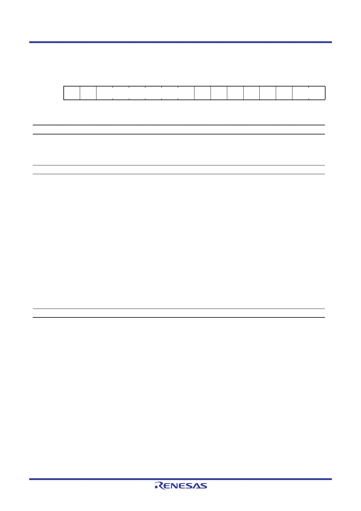
Address(es): 0008 0028h
b15 b14 b13 b12 b11 b10 b9 b8 b7 b6 b5 b4 b3 b2 b1 b0
—— STC[5:0] ——————PLIDIV[1:0]
Value after reset:
0000111100000000
Bit Symbol Bit Name Description R/W
b1, b0 PLIDIV[1:0] PLL Input Frequency
Division Ratio Select
b1 b0
0 0: ×1
0 1: ×1/2
1 0: ×1/4
1 1: Setting prohibited
R/W
b7 to b2 — Reserved These bits are read as 0. The write value should be 0. R/W
b13 to b8 STC[5:0] Frequency Multiplication
Factor Select
b13 b8
0 0 0 1 1 1: ×4
0 0 1 0 0 0: ×4.5
0 0 1 0 0 1: ×5
0 0 1 0 1 0: ×5.5
0 0 1 0 1 1: ×6
0 0 1 1 0 0: ×6.5
0 0 1 1 0 1: ×7
0 0 1 1 1 0: ×7.5
0 0 1 1 1 1: ×8
0 1 0 0 0 0: ×8.5
0 1 0 0 0 1: ×9
0 1 0 0 1 0: ×9.5
0 1 0 0 1 1: ×10
0 1 0 1 0 0: ×10.5
0 1 0 1 0 1: ×11
0 1 0 1 1 0: ×11.5
0 1 0 1 1 1: ×12
0 1 1 0 0 0: ×12.5
0 1 1 0 0 1: ×13
0 1 1 0 1 0: ×13.5
Settings other than above are prohibited.
R/W
b15, b14 — Reserved These bits are read as 0. The write value should be 0. R/W

 Loading...


