R01UH0823EJ0100 Rev.1.00 Page 1772 of 1823
Jul 31, 2019
RX23W Group 51. Electrical Characteristics
51.3.2 Reset Timing
Note 1. When OFS1.(LVDAS, FASTSTUP) bits are 11b.
Note 2. When OFS1.(LVDAS, FASTSTUP) bits are a value other than 11b.
Note 3. When IWDTCR.CKS[3:0] bits are 0000b.
Note 4. When WDTCR.CKS[3:0] bits are 0001b.
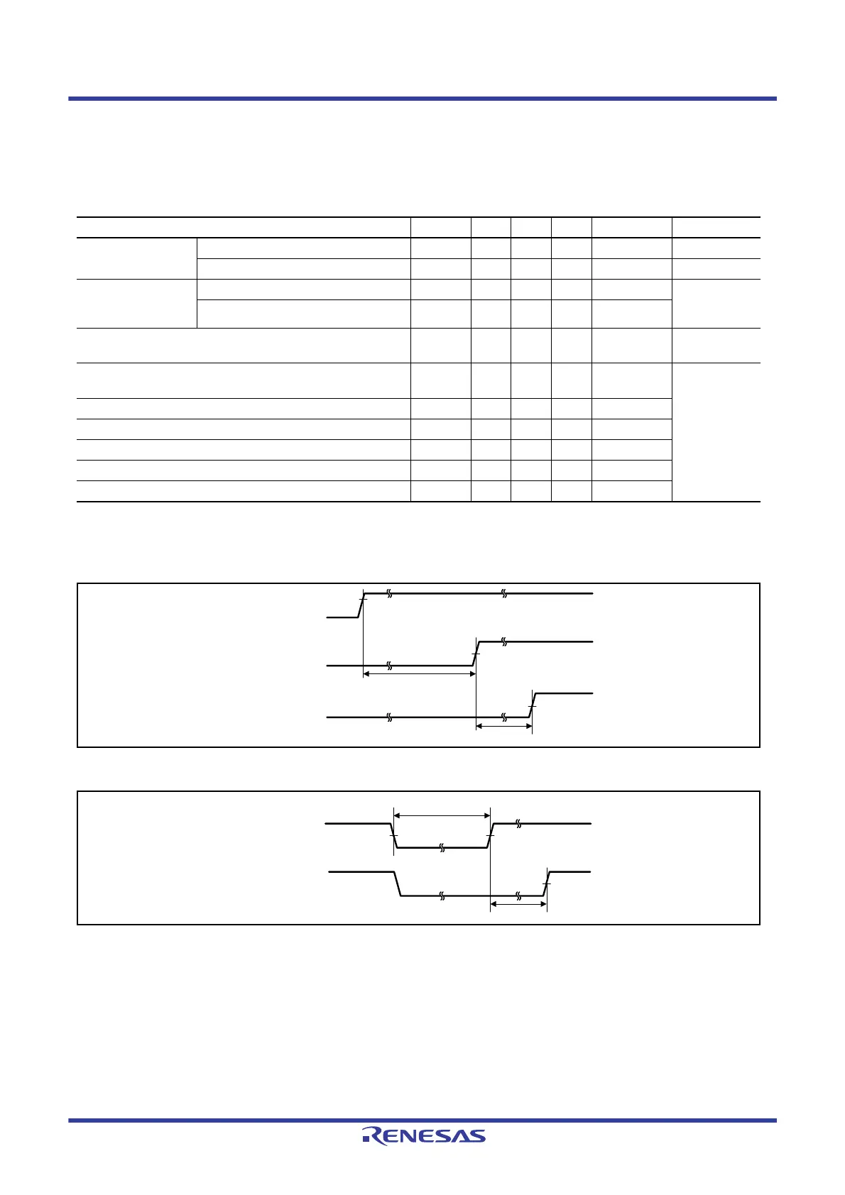
Figure 51.27 Reset Input Timing at Power-On
Figure 51.28 Reset Input Timing (1)
Table 51.25 Reset Timing
Conditions: 1.8 V ≤ VCC = VCC_USB = AVCC0 = VCC_RF = AVCC_RF ≤ 3.6 V, VSS = AVSS0 = VSS_USB = VSS_RF = 0 V,
T
a
= –40 to +85°C
Item Symbol Min. Typ. Max. Unit Test Conditions
RES# pulse width At power-on t
RESWP
3 — — ms Figure 51.27
Other than above t
RESW
30 — — μs Figure 51.28
Wait time after RES#
cancellation
(at power-on)
At normal startup*
1
t
RESWT
— 8.5 — ms Figure 51.27
During fast startup time*
2
t
RESWT
— 560 — μs
Wait time after RES# cancellation
(during powered-on state)
t
RESWT
— 120 — μs Figure 51.28
Independent watchdog timer reset period t
RESWIW
— 1 — IWDT clock
cycle
Figure 51.29
Watchdog timer reset period t
RESWWW
— 4 — PCLKB cycle
Software reset period t
RESWSW
— 1 — ICLK cycle
Wait time after independent watchdog timer reset cancellation*
3
t
RESWT2
— 300 — μs
Wait time after watchdog timer reset cancellation*
4
t
RESWT2
— 300 — μs
Wait time after software reset cancellation t
RESWT2
— 170 — μs
VCC
RES#
t
RESWP
Internal reset
t
RESWT
RES#
Internal reset
t
RESWT
t
RESW

 Loading...


