R01UH0823EJ0100 Rev.1.00 Page 226 of 1823
Jul 31, 2019
RX23W Group 11. Low Power Consumption
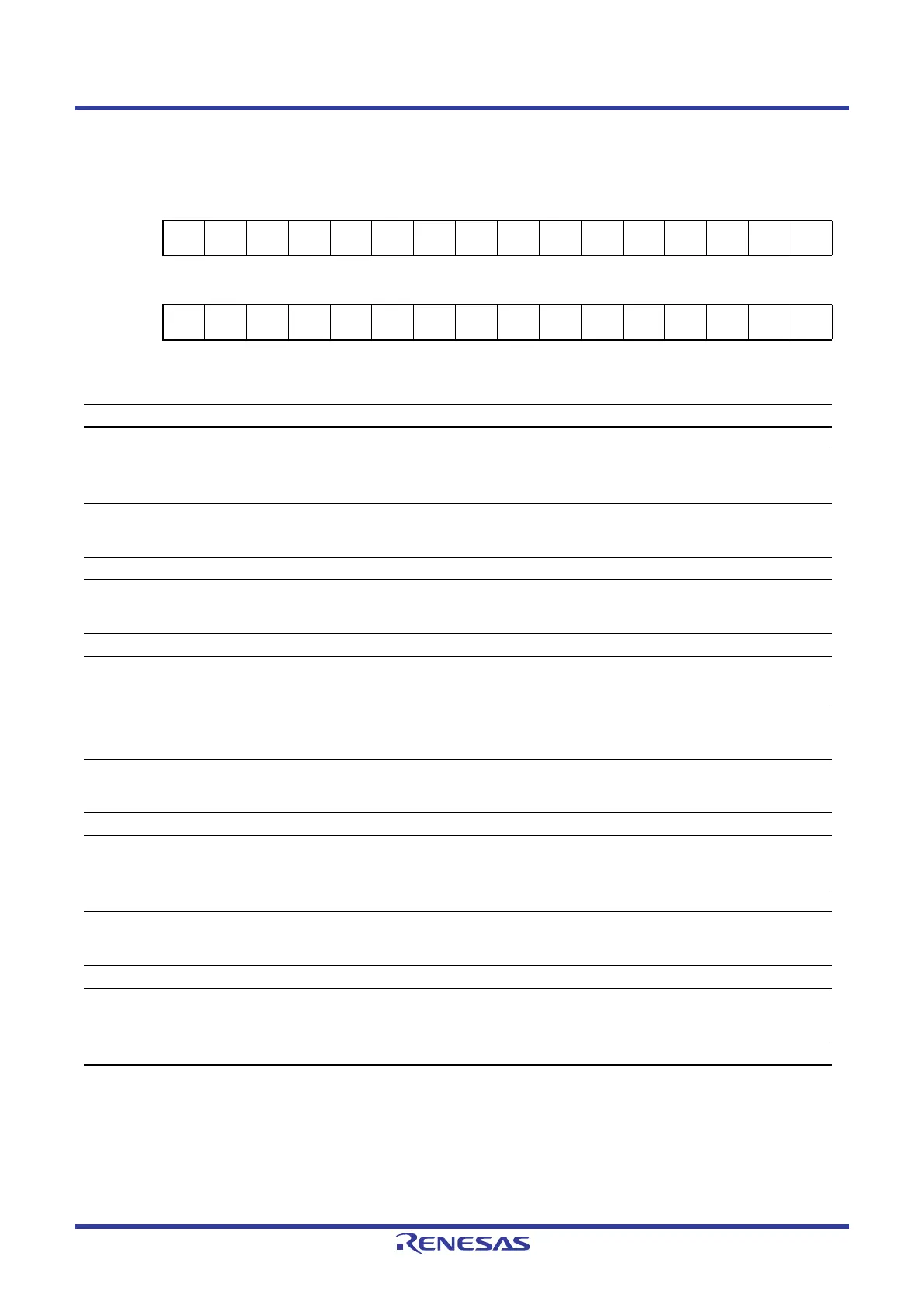
11.2.2 Module Stop Control Register A (MSTPCRA)
Note: Set the PRCR.PRC1 bit to 1 (write enabled) before rewriting this register.
Address(es): 0008 0010h
b31 b30 b29 b28 b27 b26 b25 b24 b23 b22 b21 b20 b19 b18 b17 b16
———
MSTPA
28
————————
MSTPA
19
—
MSTPA
17
—
Value after reset:
1110111111111111
b15 b14 b13 b12 b11 b10 b9 b8 b7 b6 b5 b4 b3 b2 b1 b0
MSTPA
15
MSTPA
14
MSTPA
13
———
MSTPA
9
———
MSTPA
5
MSTPA
4
————
Value after reset:
1111111111111111
Bit Symbol Bit Name Description R/W
b3 to b0 — Reserved These bits are read as 1. The write value should be 1. R/W
b4 MSTPA4 8-bit Timer 3 and 2 (Unit 1)
Module Stop
Target module: TMR3, TMR2
0: This module clock is enabled
1: This module clock is disabled
R/W
b5 MSTPA5 8-bit Timer 1 and 0 (Unit 0)
Module Stop
Target module: TMR1, TMR0
0: This module clock is enabled
1: This module clock is disabled
R/W
b8 to b6 — Reserved These bits are read as 1. The write value should be 1. R/W
b9 MSTPA9 Multifunction Timer Pulse
Unit 2 Module Stop
Target module: MTU (MTU0 to MTU4)
0: This module clock is enabled
1: This module clock is disabled
R/W
b12 to b10
— Reserved
These bits are read as 1. The write value should be 1.
R/W
b13
MSTPA13 16-Bit Timer Pulse Unit
Module Stop
Target module: TPU (TPU0 to TPU5)
0: The module stop state is canceled
1: Transition to the module stop state is made
R/W
b14
MSTPA14 Compare Match Timer 1
(Unit 1) Module Stop
Target module: CMT unit 1 (CMT2, CMT3)
0: This module clock is enabled
1: This module clock is disabled
R/W
b15 MSTPA15 Compare Match Timer
(Unit 0) Module Stop
Target module: CMT unit 0 (CMT0, CMT1)
0: This module clock is enabled
1: This module clock is disabled
R/W
b16
— Reserved
This bit is read as 1. The write value should be 1.
R/W
b17 MSTPA17 12-Bit A/D Converter
Module Stop
Target module: S12AD
0: This module clock is enabled
1: This module clock is disabled
R/W
b18 — Reserved
This bit is read as 1. The write value should be 1.
R/W
b19 MSTPA19 12-Bit D/A Converter
Module Stop
Target module: DA
0: This module clock is enabled
1: This module clock is disabled
R/W
b27 to b20
— Reserved
These bits are read as 1. The write value should be 1.
R/W
b28 MSTPA28 DMA Controller / Data
Transfer Controller Module
Stop
Target module: DMAC/DTC
0: This module clock is enabled
1: This module clock is disabled
R/W
b31 to b29 — Reserved These bits are read as 1. The write value should be 1. R/W

 Loading...


