R01UH0823EJ0100 Rev.1.00 Page 1545 of 1823
Jul 31, 2019
RX23W Group 44. 12-Bit A/D Converter (S12ADE)
44.2.8 A/D-Converted Value Addition/Average Function Select Register 0 (ADADS0)
ADADS0 selects the channels 0 to 7 on which A/D conversion is performed successively 2, 3, 4, or 16 times and then
converted values are added (integrated) or averaged.
ADS0n Bit (n = 00 to 07) (A/D-Converted Value Addition/Average Channel Select)
When the ADS0n bit of the number that is the same as that of A/D-converted channel selected by the
ADANSA0.ANSA0n bit (n = 00 to 07) or ADCSR.DBLANS[4:0] bits and ADANSB0.ANSB0n bit (n = 00 to 07) is set
to 1, A/D conversion of analog input of the selected channels is performed successively 2, 3, 4, or 16 times that is set
with the ADC[2:0] bits in ADADC. When the ADADC.AVEE bit is 0, the value obtained by addition (integration) is
stored in the A/D data register. When the ADADC.AVEE bit is 1, the mean value of the results obtained by addition
(integration) is stored in the A/D data register. As for the channel on which the A/D conversion is performed and
addition/average mode is not selected, a normal one-time conversion is executed and the conversion result is stored to the
A/D data register.
The ADS0n bit should be set while the ADCSR.ADST bit is 0.
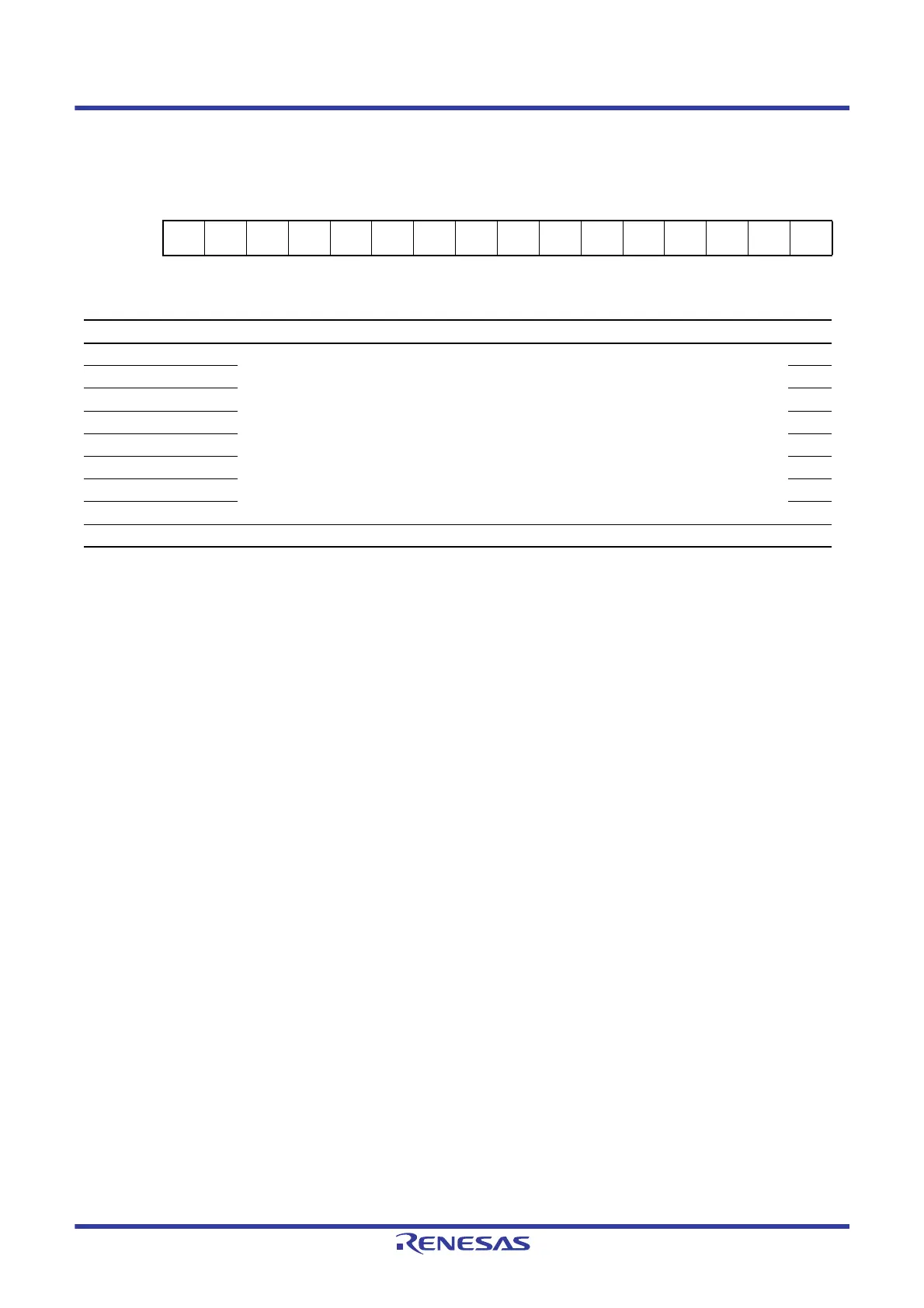
Address(es): S12AD.ADADS0 0008 9008h
b15 b14 b13 b12 b11 b10 b9 b8 b7 b6 b5 b4 b3 b2 b1 b0
————————
ADS00
7
ADS00
6
ADS00
5
ADS00
4
ADS00
3
ADS00
2
ADS00
1
ADS00
0
Value after reset:
0000000000000000
Bit Symbol Bit Name Description R/W
b0 ADS000 A/D-Converted Value Addition/
Average Channel Select
0: A/D-converted value addition/average mode for AN000
to AN007 is not selected.
1: A/D-converted value addition/average mode for AN000
to AN007 is selected.
R/W
b1 ADS001 R/W
b2 ADS002 R/W
b3 ADS003 R/W
b4 ADS004 R/W
b5 ADS005 R/W
b6 ADS006 R/W
b7 ADS007 R/W
b15 to b8 — Reserved These bits are read as 0. The write value should be 0. R/W

 Loading...


